Public info about the author: CadenceDesigner
- Profile

-

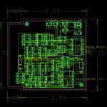
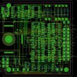
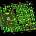
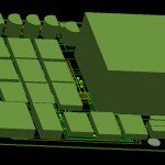
SPICE simulation PCB layout and 3D model of a 3-phase brushless DC motor driver circuit. The 3-phase power stage is composed by six power transistors, 2 PNP MJE2955 and 2 NPN MJE3055.
-

PSpice simulation of clamper and clipper circuits. These devices are diode based circuits. Clamper circuits change the DC level of an input signal, they ‘re used in voltage multipliers, capacitance meter, analog frequency meter. The clipper circuits eliminate a portion of the input signal, they ‘re used in rectifiers, voltage limiters, radar application, radio-receivers etc.
-

In this circuit is added a jfet transistor to the classic wien bridge schematic. A jfet in the feedback network let the gain vary over a small range to ensure consistent oscillation. At startup, the JFET gate voltage is zero, the drain-source impedance is very low. This produces a gain enough to get the circuit going. Once oscillations build up, the rectified negative transitions of the output provide a turn-off voltage for the JFET’s gate. This reduces the gain, and the circuit settles down to stable oscillation.
-

this voltage controlled oscillator is implemented with two operational amplifiers TL082 and a transistor NPN Q2SC1815. This device consists of three main stages. the first stage is an integrator, the second stage is a Schmitt trigger and the final stage is a NPN transistor used as switch. The input to the circuit is a DC voltage, it can range from 0.2V to 29V providing a signal frequecy from 300hz to 35khz, with a integrator capacitor fixed to 1nF.
-

This voltmeter is an integrating A/D converter, where the output represents the integral of an input voltage over a fixed period of time. the advantage of this method of measurement is in the reliable result in the presence of high frequency noise and the extremely small nonlinearity errors since it uses the time to quantize the answer. Moreover the auto-zero feature allows the manufacturer to use operational amplifiers with up to 10mV offset.
- Free
- Advanced
- 31-50
- PSpice
- 16.5+
- Yes
-
In the dual-slope technique each measurement is divided into three phases. The first phase is the auto-zero phase, where the errors in the analog components, as the offset voltage, are automatically nulled out by grounding the input and closing a feedback loop such that the error information that makes dV/dt of the integrator equal to zero is stored on the auto-zero capacitor and the reference capacitor is charged to the reference voltage Vref. In the second phase the input signal to be measured Vin, is integrated for a fixed number of clock pulses, in this case the frequency of clock is 120khz, and the integration period is 1000 clock pulses. The integrator capacitor will ramp up at a rate proportional to Vin. In the third and final phase the integrator input is switched from Vin to Vref.The integrator ramps down at a rate that is proportional to Vref. The number of clock pulses beetwen the beginning of this cycle and the time when the integrator back to its auto-zero value is a digital measure of Vin. Vin will be = (number of clock pulses)/1000 * Vref.
-


