In this article, we will examine the essential procedure for moving from a complete circuit diagram, in this case featuring a PIC microcontroller in Proteus schematic, to its associated PCB project in Proteus PCB. This step by step guide aims to provide a systematic and informative guide, to facilitate the seamless conversion of your electronic circuits into tangible and functional prototypes through the utilization of Proteus PCB
Let’s commence with this comprehensive Proteus schematic.
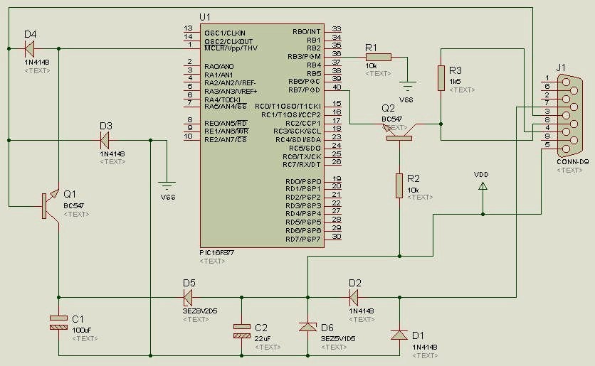
this microcontroller circuit has the following components:
4 diodes 1N4148
2 NPN transistors BC547
2 electrolitic capacitors CAP-ELEC
2 zener diodes a 3EZ8V2D5 and a 3EZ5V1D5
3 resistors RES
a connector D-type 9 pin female CONN-D9
a PIC microcontroller PIC16F877
The PIC16F877 features two concealed pins, VDD and VSS. The VDD pin should be designated as ‘POWER,’ and the VSS pin should be assigned as ‘GROUND.’ When incorporating a component in Proteus Schematic, certain components are preconfigured with a corresponding PCB footprint, while others may not possess an associated PCB footprint and necessitate manual addition. In such instances, it is imperative to manually include the appropriate footprint, as illustrated in the ‘CAP-ELEC’ example below:
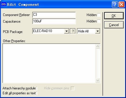
Open the Properties dialog box for the CAP-ELEC component. Click the “?” Button (in the latest versions the binoculars icon) to open the PCB package selection dialog
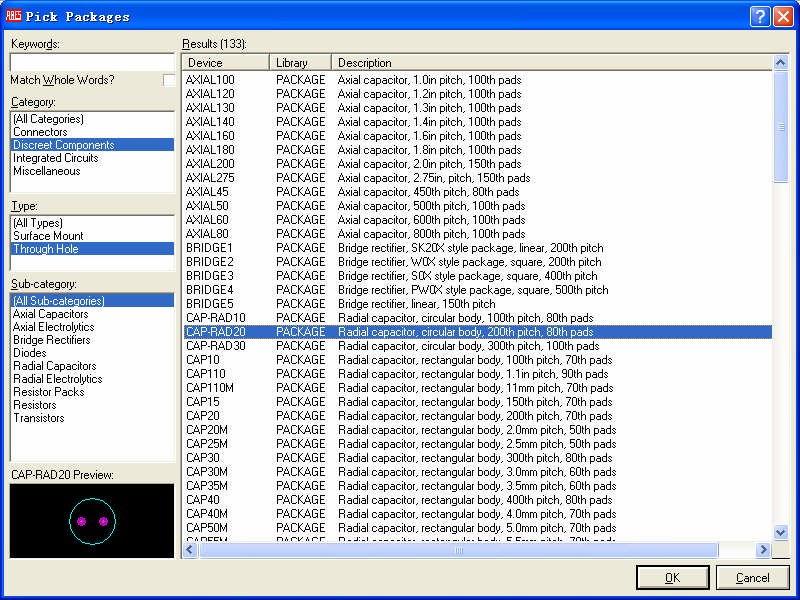
Select an appropriate PCB footprint, and then click ‘OK’ to confirm your choice. Proceed to select PCB footprints for all the components. Next, open the Netlist Compiler by navigating to the ‘Tools’ menu within Isis Proteus (Tools -> Netlist Compiler). A settings dialog box will appear; please retain the default settings and click ‘OK’ to generate the netlist file. Once the file is generated, access ARES software by selecting ‘Tools -> Netlist to ARES’ from the ‘Tools’ menu. Alternatively, you can utilize the corresponding button on the toolbar to perform this operation.
Note: in the latest versions of Proteus it is sufficient to click on the PCB Layout icon:

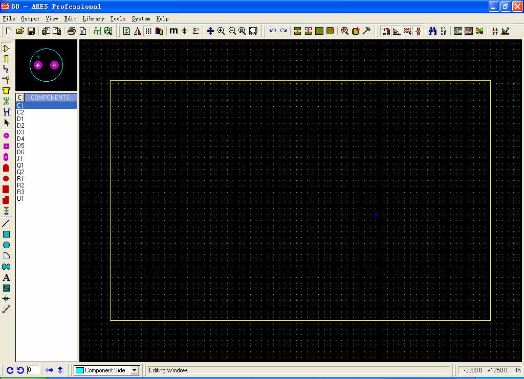
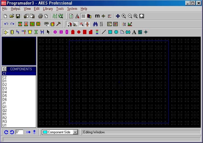
As we can see, the workspace is currently empty, and our intention is to utilize all the elements listed on the left.
Before proceeding with component placement, it is essential to create a border. To achieve this, we utilize the ‘2D Graphics Box Mode’ button to draw the border:
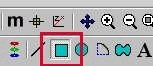
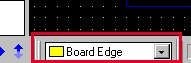
Prior to initiating the drawing procedure, it is necessary to make a color selection. Given the border’s nature, we have chosen the color yellow (Board Edge), as discernible within the settings tool situated at the lower section of the main window:
Click within the workspace, hold down the left mouse button, drag the cursor to define a rectangle of suitable dimensions, and then release the mouse button.
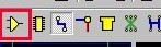
If you wish to make adjustments to the board’s size at a later stage, you can follow these steps: Click on the ‘2D Graphics Box’ rectangular icon once more, right-click on any of the board’s corners to reveal a control point, and then drag this control point to resize the board. To return to the components placement view, simply click the icon located below:
To populate the board with components, please follow these steps. For an overall perspective, press the ‘F8’ key. The outcome will be as follows: