Public info about the author: Cribald
- Profile
- Electronics engineer graduated at Università Politecnica delle Marche in Ancona. Experience in software and hardware designing. PSpice user since the days of university studies.

-

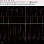
This simulation with OrCAD PSpice 16.6 , shows a simple and elegant method to analyze the stability of a 3-stage amplifier with feedback applied as the compensation capacitors vary. This method is applied to the 200 Watt Mosfet Power Amplifier AL-35.
We ‘ll see how to estimate the phase margin with Bode diagrams and how the compensation capacitors affect the phase margin and the frequency response of the amplifier gain. -
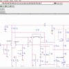
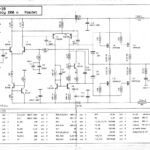
Spice simulation with OrCAD PSpice of a 200Watt Power mosfet amplifier Zestaw AL-35. A 3 stage power amplifier with 2 N-channel Mosfet IRFP240 and 2 P-channel IRFP9240. IRFP9240 models in IRF and PWRMOS libaries are not suitable for performing the simulation correctly, new IRFP9240 models have been imported
.The BD139 NPN transistor model and the medium power PNP transistor MJE350 model are missing in the default PSpice libraries. All the models are inside the .zip file. For adding all .lib and .olb libraries read the readme.txt file. -

A complete course using PSpice as SPICE simulator for a practical and easy way to learn 3-stage audio power amplifiers design with theory and SPICE simulation analysis. You ‘ll learn to calculate and size components of a basic three stage power amplifier. The sources current circuits of the first stage, study the effects of a feedback signal application, the mirroring of the first stage currents, design of a typical dual rail power supply for a fixed power, features of enhanced output stages with a current limiter, a zobel network filter, Nyquist Criterion to validate the stability of the amplifier with a feedback applied. The course explains how to implement frequency compensation with one or two dominant poles with compensation capacitors, design of top quality BJT 100W quasi complementary class B, 100W complementary class B, 140W class B, 40W class A.
- For-Credits
- Advanced
- >100
- PSpice
- 9.2
- Yes
-
COURSE CONTENTS:
"What you will learn from the course:"
1) "The Basic Schematic underlying all 3-stage amplifiers with applied feedback.":
The basic schematic of a 3-stage amplifier with applied feedback consists of three amplification stages interconnected in a specific configuration. Each stage performs a specific amplification function to boost the input signal.
2) "How to implement a current mirror in a BJT amplifier."
A current mirror in a BJT audio amplifier is a circuit configuration used to replicate or mirror the current flowing through one transistor onto another transistor. It consists of two or more transistors arranged in a specific configuration to ensure that the collector current of one transistor precisely matches the collector current of another transistor.
3) "How to design an enhanced output stage to make the final transistors operate within their safe operating region."
You 'll understand how to implement a single or double slope circuit that allows the final transistors to operate in a safe region and compensate the reactive behavior that the speakers can exhibit"
4) "How to design a typical dual power supply for the 3-stage amplifier.":
A dual power supply for a 3-stage BJT amplifier refers to a power configuration that provides positive and negative voltage rails to the amplifier circuit.
The purpose of a dual power supply is to enable the amplifier to handle both positive and negative signals, ensuring symmetrical operation and allowing for amplification of AC signals that swing above and below the reference ground level.5) "How to verify the stability of a 3-stage amplifier and how to intervene to improve the stability of the amplifier with applied feedback."
The Nyquist criterion assesses the stability by analyzing the frequency response and the open-loop gain of the amplifier.
Plot the Nyquist diagram using the open-loop transfer function. Identify the gain and phase margins from the Nyquist plot. Compare the gain and phase margins with the desired specifications. Adequate margins ensure stability and reliable performance.6) "The schematic of a quasi-complementary 100W Class B amplifier."
The notable feature of this topology is that the output stage is asymmetrical, consisting of only ONE complementary pair of NPN and PNP transistors.
7) "The schematic of a complementary 100W Class B amplifier."
amplifier with a COMPLEMENTARY configuration in the OUTPUT STAGE, with two complementary pairs of NPN-PNP transistors
8) "Schematic of a 140W Class B amplifier."
Class B amplifier qith EMITTER FOLLOWER OUTPUT STAGE WITH PARALLEL FINAL DEVICES
9) "Schematic of a high-performance, very low-distortion 40W Class A amplifier."
A Class A amplifier that incorporates all the advanced features seen in previous amplifiers to ensure a very high level of performance, such as current mirrors, stabilized current sources, double slope circuits in the output stage, parallel final transistors.compensation circuit for potential reactive behavior of the speakers."
The simulated schematics have a descriptive section that explains the operation of each component and how to perform the design calculations.
You will have ready-to-simulate schematics available that can be customized according to your needs.
Along with the course on 3-stage amplifier with BJT, you will find the Course on BJT, JFET, and MOSFET transistors, a course to learn how to optimally use these devices both as signal amplifiers and switches.
COURSE CONTENTS:
Ic - Vce CARACHTERISTIC OF TRANSISTOR BJT NPN
SINGLE STAGE BJT COMMON EMITTER
SINGLE STAGE BJT COMMON EMITTER WITH EMITTER CAPACITOR
SINGLE STAGE BJT COMMON BASE
SINGLE STAGE BJT COMMON COLLECTOR
BIASING BJT NPN WITH ONLY 2 RESISTORS
BIASING BJT NPN WITH 3 RESISTORS
BIASING BJT NPN WITH 4 RESISTORS
BIASING BJT PNP WITH 4 RESISTORS
BIASING BJT NPN WITH FEEDBACK RESISTOR
TRANSISTOR BJT NPN AS SWITCH
TRANSISTOR BJT PNP AS SWITCH
BIASING COMMON BASE BJT WITH TWO VOLTAGE SOURCES
TWO STAGE BJT NPN COMMON EMITTER
TWO STAGES BJT NPN COMMON EMITTER WITH EMITTER CAPACITORS
CHARACTERISTIC Id - Vgs OF JFET N-CHANNEL
BIASING OF N-CHANNEL JFET
BIASING P-CHANNEL JFET
JFET N-CHANNEL AS SWITCH
SINGLE STAGE FET COMMON SOURCE
SINGLE STAGE FET COMMON SOURCE WITH SOURCE CAPACITOR
BIASING N-CHANNEL JFET WITH 4 RESISTORS
CHARACTERISTIC ID-VGS OF ENHANCE MODE MOSFET N CHANNEL
BIASING OF ENHANCED MODE MOSFET N-CHANNEL WITH FEEDBACK RESISTOR
BIASING ENHANCEMENT MOSFET N-CHANNEL WITH 4 RESISTORS
CHARACTERISTIC ID-VGS OF DEPLETION MODE MOSFET N CHANNEL
BIASING DEPLETION MODE MOSFET N-CHANNEL WITH 4 RESISTORSAdding this Course will enhance your experience even further, especially if you're not already familiar with how to bias the transistors for their optimal usage.
-


-

SPICE simulation of a very high quality BJTs power amplifier in class A. Three stages, class A amplifier, double simmetrical differential couple with current mirrors. Sources currents with automatic control of the constant current amplitude. Feedback circuit and couple of compensation capacitors for every differential couple of the first stage. Darlington and cascode configuration transistors in the intermediate stage. Complementary parallel final transistors in emitter follower configuration, and SOAR circuit with double slope limiter circuit.
-

SPICE simulation of a an active low pass filter in voltage follower configuration. How sizing the component values to set the cutoff frequency.

