Public info about the author: JacobBaker
- Profile
- Professor in the Electrical and Computer Engineering department at Boise State University, member of the electrical engineering honor society Eta Kappa Nu, a licensed Professional Engineer

-

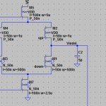
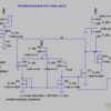
SPICE simulation of 1 Gbit/s clock recovery circuit using a NRZ (Non Return to Zero) data format. The Digital Phase Locked Loops used for clock recovery uses a Hogge phase detector and a VCDL (Voltage Controlled Delay Line), the output of which is fed back to get a positive feedback for sustaining the oscillation.
- Free
- Advanced
- >100
- LTspice
- IV
- No
-


-
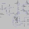
SPICE simulation of the Digital Delay Loop (DDL) that uses the modified version of Voltage-Controlled Delay Line (VCDL). The VCDL gain must be as linear as possible, otherwise the DLL can exhibit second-order locking effects. To reduce the jitter and to linearize the loop’s response, a large capacitor (5pF) is used for the loop filter.
- Free
- Advanced
- 51-100
- LTspice
- IV
- No
-

-

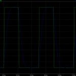
SPICE simulation of a modified VCDL. This version of Voltage-Controlled Delay Line regenerates full logic levels without introducing distortion into the signals. In this VCDL has been changed the last stage to two diff-amps with swapped input signals. The resulting signals have a width greater than the unmodified version. To get full logic levels, signals pass through inverters.
- Free
- Advanced
- 51-100
- LTspice
- IV
- No
-


-

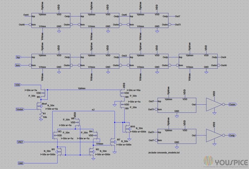
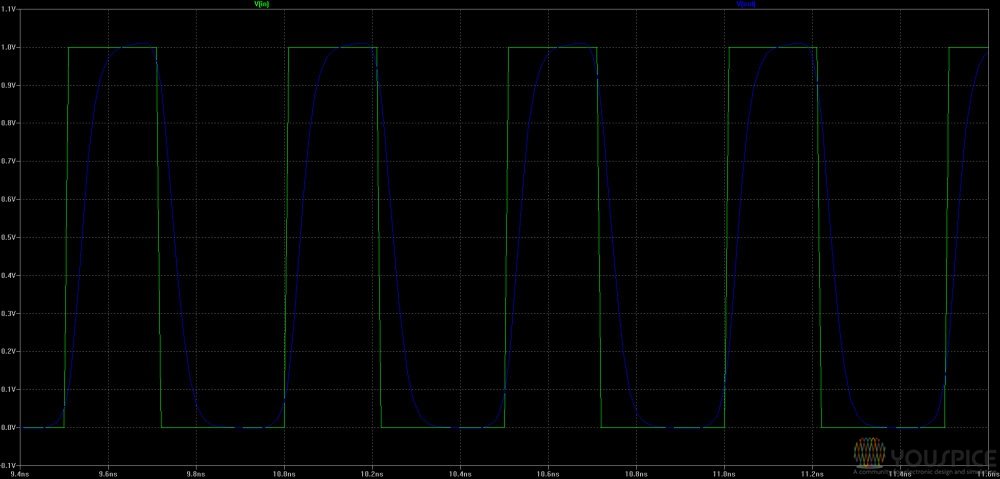
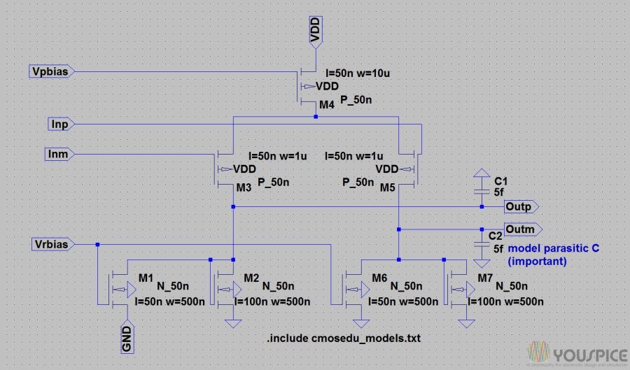
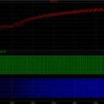
SPICE simulation of an 8 stage voltage controlled delay line. The VCDL is used to provide delay in a delay locked loop (DLL). This schematic has eight delay cells. The differential inputs were generated using an inverter and a transmission gate. The outputs are evenly spaced and they only swing up to Vref = 500mV. This is done to minimize the effects of power supply and ground noise on the delay of the circuit.
- Free
- Advanced
- 51-100
- LTspice
- IV
- No
-


-
Problems with PLL output jitter resulting from the VCO output frequency changing with a constant input voltage (VjnVC0 = constant) has led to the concept of a delay-locked loop (DLL). Assuming that a reference clock is available at exactly the correct frequency, the input data is delayed through a voltage-controlled delay line (VCDL) a time t0 until it is synchronized with the reference clock. Jitter is reduced by using an element, the VCDL, that does not generate a signal (like the VCO does). The transfer function Fclock/Fout is zero (the phase of the reference clock is taken as the reference for the other signals in the DLL, i.e., Fclock = 0), so that oscillator noise and the resulting jitter are not factors in DLL design.
- Free
- Intermediate
- 11-20
- LTspice
- IV
- No
-