Description
Ic-Vce characteristic of BJT, Id-Vgs characteristic of JFET.BJT and JFET as switches.Biasing BJT with 2 resistors, 3 resistors, feedback resistor, 4 resistors.Single stage BJT common base, common emitter, common collector, common emitter with emitter capacitor.Multistage BJT common emitter, multistage BJT common emitter with emitter capacitor.Biasing N-channel JFET, biasing P-channel JFET, single stage JFET common source, single stage JFET common source with source capacitor.Biasing enhancement MOSFET N-channel with 4 resistors and with feedback resistor.Biasing depletion mode MOSFET N-channel with 4 resistors.
- For-Credits
- Intermediate
- >100
- PSpice
- 9.1+
- No
-
Course on BJT, JFET, and MOSFET transistors, a course to learn how to optimally use these devices both as signal amplifiers and switches.
COURSE CONTENTS:
Ic - Vce CARACHTERISTIC OF TRANSISTOR BJT NPN
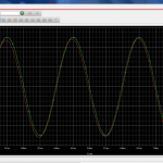
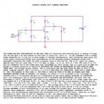
SINGLE STAGE BJT COMMON EMITTER
SINGLE STAGE BJT COMMON EMITTER WITH EMITTER CAPACITOR
SINGLE STAGE BJT COMMON BASE
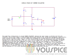
SINGLE STAGE BJT COMMON COLLECTOR
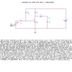
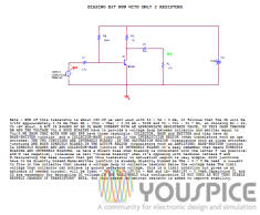
BIASING BJT NPN WITH ONLY 2 RESISTORS
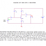
BIASING BJT NPN WITH 3 RESISTORS
BIASING BJT NPN WITH 4 RESISTORS
BIASING BJT PNP WITH 4 RESISTORS
BIASING BJT NPN WITH FEEDBACK RESISTOR
TRANSISTOR BJT NPN AS SWITCH
TRANSISTOR BJT PNP AS SWITCH
BIASING COMMON BASE BJT WITH TWO VOLTAGE SOURCES
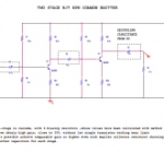
TWO STAGE BJT NPN COMMON EMITTER
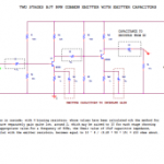
TWO STAGES BJT NPN COMMON EMITTER WITH EMITTER CAPACITORS
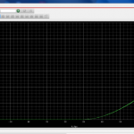
CHARACTERISTIC Id - Vgs OF JFET N-CHANNEL
BIASING OF N-CHANNEL JFET
BIASING P-CHANNEL JFET
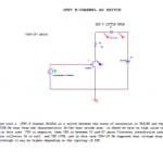
JFET N-CHANNEL AS SWITCH
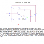
SINGLE STAGE FET COMMON SOURCE
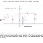
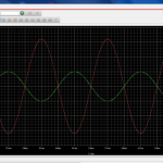
SINGLE STAGE FET COMMON SOURCE WITH SOURCE CAPACITOR
BIASING N-CHANNEL JFET WITH 4 RESISTORS
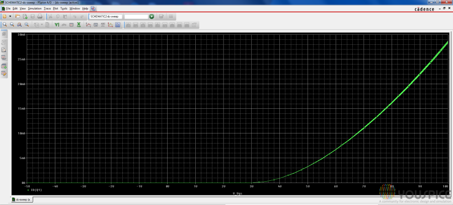
CHARACTERISTIC ID-VGS OF ENHANCE MODE MOSFET N CHANNEL
BIASING OF ENHANCED MODE MOSFET N-CHANNEL WITH FEEDBACK RESISTOR
BIASING ENHANCEMENT MOSFET N-CHANNEL WITH 4 RESISTORS
CHARACTERISTIC ID-VGS OF DEPLETION MODE MOSFET N CHANNEL
BIASING DEPLETION MODE MOSFET N-CHANNEL WITH 4 RESISTORSWith this Course will enhance your experience on these devices, especially if you're not already familiar with how to bias the transistors for their optimal usage.
P.S.
If running simulation you get undefined error message, go to menu PSpice/Edit Simulation Profile, Configuration Files TAB, Category: library, and add to design libraries .lib embedded in files project.
Pay attention: in a multiple design, to switch between projects, on FILE tab go to PSpice Resources, Simulation Profiles,
click on the project, dx mouse button and select "make active". -




















Reviews
There are no reviews yet.