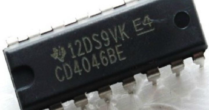
The CD4046 is an electronic component that belongs to the family of CMOS integrated circuits (Complementary Metal-Oxide-Semiconductor). It is a PLL (Phase-Locked Loop), which is a feedback control system with the capability to synchronize the phase of an output signal with that of a reference input signal. This component is primarily used in analog and digital electronic applications to generate, demodulate, synchronize, and modulate signals. After a brief overview of the component, the CD4046 SPICE model will be presented, offering comprehensive insights into its behavior and characteristics.
The CD4046 is primarily composed of three fundamental parts:
- VCO (Voltage-Controlled Oscillator): This section generates an oscillating signal whose frequency is controlled by the control voltage. The output frequency is directly proportional to the input voltage, making it useful for generating variable-frequency signals.
- Phase Detector: This part of the circuit compares the phase of the input signal with that of the feedback signal from the VCO output. Any phase difference between these two signals generates an error signal used to adjust the VCO frequency, ensuring that the phase of the output signal aligns with that of the input signal.
- Divider: This section includes division circuits that can be used to divide the frequency of the input signal or the feedback signal. This division can be useful for achieving desired frequency ratios in the synchronization process.
The main uses of the CD4046 include:
Frequency Demodulation:
The CD4046 can be used to demodulate frequency-modulated (FM) signals by converting them into voltage signals. This is useful in applications such as receiving FM radio signals.
Variable-Frequency Signal Generation:
Thanks to the VCO, the CD4046 can generate output signals with a variable frequency controlled by a voltage. This is useful in musical synthesizers, testing instruments, and other applications where generating variable-frequency signals is necessary.
Phase Detection:
The CD4046 can be used to detect phase differences between two signals. This is valuable in electronic control systems, optical alignment systems, and other applications where phase synchronization is important.
Frequency Tracking:
It can be used to monitor frequency variations in an input signal and generate an output signal proportional to these variations. This can be beneficial in frequency control applications.
Now let’s take a look at the CD4046 SPICE model:
.subckt CD4046 sigin phcmpii phcmpi phpls compin vcoin
+ r1 r2 ce1 ce2 vcoout demout inhibit zener vdd vss
+ OPTIONAL: DPWR=$G_DPWR DGND=$G_DGND
+ PARAMS: MNTYMXDLY=0 IO_LEVEL=0
+ Rin=1Meg S1=1 S2=0.5 M1=0.5 M2=1.0 Vx=10
+ Kb=1 Vfree=0.0 Kc=-0.1 Vt=1.2 Vxqr=10
* Rin = VCO Input Resistace
* S1 = Voltage Limiter linear slope
* S2 = Voltage Limiter non-linear slope
* Vx = Input threshold voltage (between S1 and S2)
* Kb = Arbitrary constant to adjust the value of the conversion gain (transimpedance gain)
* Vfree= Frequency dependent constant in Emult
* Kc = Negative inverse amplitude of the square wave
* Vt = Trigger voltage of Schmitt trigger (not used)
* Vxqr = Amplitude of square wave (not used)
* M1 = Current mirror multiplier to adjust oscillator frequency
* M2 = Current mirror multiplier to adjust oscillator frequency
*The provided portion of the CD4046 SPICE model defines a subcircuit with the following parameters:
* r1, r2, ce1, ce2, vcoout, demout, inhibit, zener, vdd, vss are the subcircuit component nodes.
*Optional parameters are DPWR and DGND.
*Parameters are set with values: MNTYMXDLY=0, IO_LEVEL=0, Rin=1Meg, S1=1, S2=0.5, M1=0.5, M2=1.0, *Vx=10, Kb=1, Vfree=0.0, Kc=-0.1, Vt=1.2, Vxqr=10.
* Preliminary model still under development based on Natinal Semiconductor CD4046BM
* RAPerez 9/98
* Phase detector section
U1 INVA(4) DPWR DGND sigin compin isigin icompin
+ isigin icompin clk1 clk2
+ INVA_TIMING IO_HCT
+ MNTYMXDLY={MNTYMXDLY} IO_LEVEL={IO_LEVEL}
.MODEL INVA_TIMING UGATE
U2 XOR DPWR DGND isigin icompin xorout
+ XOR_TIMING IO_HCT
+ MNTYMXDLY={MNTYMXDLY} IO_LEVEL={IO_LEVEL}
.MODEL XOR_TIMING UGATE
***tplhty=20n tphlty=20n
U3 NAND(2) DPWR DGND q1 q2 pclr
+ NAND_TIMING IO_HCT
+ MNTYMXDLY={MNTYMXDLY} IO_LEVEL={IO_LEVEL}
.MODEL NAND_TIMING UGATE (tplhty=1n tphlty=1n)
U4 DFF(1) DPWR DGND $D_HI clr clk1 $D_HI q1 qb1
+ DFF1_TIMING IO_HCT
+ MNTYMXDLY={MNTYMXDLY} IO_LEVEL={IO_LEVEL}
.MODEL DFF1_TIMING UEFF tppcqlhty=4n tppcqhlty=4n tpclkqlhty=4n tpclkqhlty=4n
U5 DFF(1) DPWR DGND $D_HI clr clk2 $D_HI q2 qb2
+ DFF2_TIMING IO_HCT
+ MNTYMXDLY={MNTYMXDLY} IO_LEVEL={IO_LEVEL}
.MODEL DFF2_TIMING UEFF tppcqlhty=5n tppcqhlty=5n tpclkqlhty=5n tpclkqhlty=5n
U7 BUFA(2) DPWR DGND fq1 fq2 s1 s2
+ BUFA_TIMING IO_HCT
+ MNTYMXDLY={MNTYMXDLY} IO_LEVEL={IO_LEVEL}
.MODEL BUFA_TIMING UGATE
ST2 vdd phcmpii s1 0 swt
SB2 phcmpii vss s2 0 swt
.model swt VSWITCH (ROFF=2G RON=10m VOFF=0.8 VON=3.0)
U6 AND(2) DPWR DGND pclr reset clr
+ AND_TIMING IO_HCT
+ MNTYMXDLY={MNTYMXDLY} IO_LEVEL={IO_LEVEL}
.MODEL AND_TIMING UGATE
Ureset STIM(1,1) DPWR DGND
+ reset
+ IO_HCT
+ +0s 0
+ 2ns 1
+ 1s 1
U8 NOR(2) DPWR DGND fq1 fq2 norout
+ NOR_TIMING IO_HCT
+ MNTYMXDLY={MNTYMXDLY} IO_LEVEL={IO_LEVEL}
.MODEL NOR_TIMING UGATE
U9 ANDA(2,2) DPWR DGND q1 od1 q2 od2 fq1 fq2
+ ANDA_TIMING IO_HCT
+ MNTYMXDLY={MNTYMXDLY} IO_LEVEL={IO_LEVEL}
.MODEL ANDA_TIMING UGATE
U10 DLYLINE DPWR DGND q1 od1
+ DLY_TIMING IO_HCT
+ MNTYMXDLY={MNTYMXDLY} IO_LEVEL={IO_LEVEL}
U11 DLYLINE DPWR DGND q2 od2
+ DLY_TIMING IO_HCT
+ MNTYMXDLY={MNTYMXDLY} IO_LEVEL={IO_LEVEL}
.MODEL DLY_TIMING UDLY dlyty=12n
U12 BUFA(3) DPWR DGND norout xorout vcosqr phpls phcmpi vcoout
+ BUFB_TIMING IO_HCT
+ MNTYMXDLY={MNTYMXDLY} IO_LEVEL={IO_LEVEL}
.MODEL BUFB_TIMING UGATE
* The above portion of CD4046 SPICE model represents various sections of the circuitry within the component:
*Phase Detector Section: This section encompasses multiple subcircuits and models to simulate the behavior of the phase detector *and related components. These include logic gates like NAND, XOR, D-type flip-flops, AND, BUFA, ANDA, DLYLINE, and BUFB. *Each subcircuit is configured with specific timings and parameters for accurate simulation.
*Logic Gates: Different logic gates are utilized to implement the functionality of the phase detector. These gates include NAND, *XOR, AND, BUFA, ANDA, etc., each having their specific timing and connectivity configurations.
*Switch Model: The model “swt” represents a voltage-controlled switch. It’s used to simulate the switching behavior in the circuit.
*Stimulus Source: A stimulus source named “Ureset” generates a reset signal for simulation purposes. It provides an initial value of *0, switches to 1 after 2 nanoseconds, and maintains 1 from that point onward.
*Timing Models: Various subcircuits (NAND_TIMING, DFF1_TIMING, DFF2_TIMING, BUFA_TIMING, etc.) are configured with *specific timing parameters to accurately replicate the behavior of the corresponding logic components.
*Model Parameters: The models are configured with parameters such as “MNTYMXDLY” and “IO_LEVEL” to adjust the simulation *behavior as needed.
* VCO Section
Rin vcoin vss {Rin}
Evlim vlim 0 value={if(v(vcoin,vss)<v(vdd,vss),
+ S1*v(vcoin,vss),S2*(v(vcoin,vss)-v(vdd,vss))+v(vdd,vss))}
Rvlim vlim 0 1Meg
Emult mix 0 value={v(vlim)*Kb+Vfree}
*Hmult mix 0 poly(1) Vcm 1.44 0.586
Rmult mix 0 1
Edemout demout 0 table={ 200Meg*v(vcoin,demout)*v(off) } (-20,-20) (20,20)
Rdemout demout 0 1Meg
ER2 ir2 0 vdd ir2 200Meg
VR2 ir2 r2
ER1 ir1 0 mix ir1 200Meg
VR1 ir1 r1
Eosclg adj 0 table={abs((V(vdd)/I(VR2))/(V(mix)/I(VR1)))}
+ (0.5,1.43) (1,1.6) (10,1.04) (50,0.67) (100,0.84) (101,1)
+ (102,1) (1000,1)
Radj adj 0 1G
*GIM ce1 0 value={(M1*I(VR1)+M2*I(VR2))*Kc*V(sqrrc)}
GIM ce1 0 value={(M1*I(VR1)*V(adj)+M2*I(VR2))*Kc*V(sqrrc)}
*GIM ce1 0 value={(24*I(VR1)+3.067*I(VR2))}
Vcext ce2 0
Cstray ce1 ce2 6p
Rcext ce1 ce2 1T
Etrngl trngl 0 ce1 0 1
Rtrngl trngl 0 1Meg
Esqr sqr 0 value={-10Meg*V(trngl)+1.2Meg*V(sqrrc)}
Rsqr sqr sqrrc 0.1T
Csqr sqrrc 0 10f
Dsqr1 sqrrc 13 Diode
Vsqr1 13 0 {Vx}
Dsqr2 14 sqrrc Diode
.model Diode D (IS=10u N=0.1 CJO=80f RS=1m)
*.model Diode D (IS=10u N=0.001 CJO=80f)
Vsqr2 14 0 {-Vx}
Ipls 0 sqrrc pwl 0 0 10n 0 20n 0.01u 0.1u 0.01u 0.12u 0 1 0
Evcoout vcosqr 0 table={5.0*v(off)*(v(sqrrc)/Vx)} (0.1,0.1) (4.5,4.5)
*Rvcoout vcosqr vcosqr1 1
**Et 7 0 TABLE {-10k*V(trngl)+1.2k*V(sqrrc)} (-2,-10) (2,10)
*Ipls 0 sqrrc pwl 0 0 10n 0 20n 1u 0.1u 1u 0.12u 0 1 0
*Et 7 0 value={table({-10Meg*V(trngl)+1.2Meg*V(sqrrc)},-10,{-Vx},10,{Vx})}
*Ro 7 sqrrc 100
*Co sqrrc 0 100p
*Est sqrrc o VALUE={table({2000k*(V(st)-V(trngl))},-2,{-Vx},2,{Vx})}
*Rst1 sqrrc st 8.8k
*Rst2 st 0 1.2k
*Cst st 0 200p ic=-10
Rinhbt inhibit 0 1Meg
Eoff off 0 value={if(v(inhibit)<0.9,1.0,0.0)}
Roff off 0 1Meg
Dzener vss zener znr
Rzener vss zener 1G
.model znr D(Is=1.004f Rs=.5875 Ikf=0 N=1 Xti=3 Eg=1.11 Cjo=160p M=.5484
+ Vj=.75 Fc=.5 Isr=1.8n Nr=2 Bv=5.2 Ibv=27.721m Nbv=1.1779
+ Ibvl=1.1646m Nbvl=21.894 Tbv1=176.47u)
.ends
This portion of the CD4046 SPICE model describes the “VCO Section” of the circuit. It includes various components and their connections that are responsible for controlling the Voltage-Controlled Oscillator (VCO) behavior within the CD4046:
- Rin and vcoin are connected to set the VCO input resistance.
- The section involving Evlim calculates the voltage limit for the VCO input signal based on specified conditions.
- Rvlim defines the resistance for voltage limiting.
- Emult calculates the multiplication of the voltage limit and a constant, along with Rmult representing resistance for multiplication.
- Edemout and Rdemout define components for generating the demodulated output signal.
- Eosclg calculates a frequency dependent constant, utilizing the adjacent voltage.
- Various components like Radj, GIM, Vcext, Cstray, Rcext, Etrngl, Rtrngl, Esqr, Rsqr, Csqr, Dsqr1, Vsqr1, Dsqr2, Vsqr2 further shape and process the VCO output signal.
- Ipls generates a piece-wise linear current source.
- Evcoout calculates the voltage of the VCO output signal.
- The section involving Dzener and Rzener defines a diode and resistor for zener voltage regulation.
- The .model znr part provides model parameters for the zener diode.
This portion of the SPICE model focuses on the detailed components and connections that constitute the VCO section of the CD4046, enabling simulation and analysis of its behavior in various scenarios.
You can find the datasheet of this component available for download Here.
How would I assign pins to the arbitrary circuit in MultiSim?
Non sono esperto di Multisim ed ho anch’io una richiesta:
Per favore qualcuno mi può indicare come inglobare CD4046 SPICE Model in LTspice?
Pierre
Per favore qualcuno sa indicarmi come inglobare CD4046 SPICE Model in LTSpice?
Hi,
Has anyone cross-checked and verified this model?
How can I employ this model of CD4046 in LTSpice?
Thanks and Regards, Ajay