Quick Solutions to Solve SPICE Convergence Issues.

This article delves into the critical subject of to Solve SPICE Convergence Issues. The solutions presented for addressing convergence issues are of a general nature and are applicable across various algorithms, such as PSPice, XSPICE, NGSPICE, IsSPICE, and HSPICE. By understanding and effectively managing convergence challenges in SPICE simulations can enhance the reliability and accuracy of their electronic circuit analyses, regardless of the specific SPICE variant they are utilizing.

Convergence problems in SPICE simulations primarily manifest in three distinct categories:

  • Circuit Topology Errors

The SPICE simulation software frequently signals these types of errors with precise messages, rendering their identification and rectification relatively straightforward.

  • SPICE simulator Options Settings

For instance, during transient analysis, selecting an appropriate timestep corresponding to the device’s operational frequency becomes very important. At times, a compromise between accuracy and convergence stability is required; as accuracy is increased, the likelihood of encountering convergence errors also rises.

  •  Unrealistic SPICE models

Convergence problems can stem from SPICE models characterized by significant nonlinearities and discontinuities. Such models introduce complexities that can challenge the simulation’s convergence process.
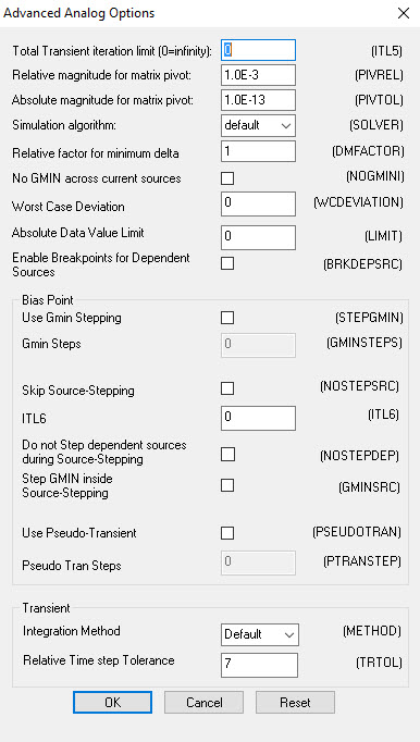
Advanced SPICE options window in PSpice

Now, let’s delve into the strategies that swiftly address the most prevalent convergence challenges arising from these distinct problem categories in order to effectively solve SPICE convergence issues.

Circuit Topology Errors

Ground Absence, Error Message: Node is Floating.

The SPICE algorithm computes voltage for every circuit point relative to a reference point—this reference point is specifically the ground, an essential component in the circuit. Including the ground reference wherever needed suffices to address this issue.

Lack of Direct DC Ground Path, Error Message: Node is Floating.

Building on the insights from the prior scenario, it’s essential to verify the absence of circuit points isolated from the ground reference. If an apparent isolation is intended for a node from the ground, this can be achieved by introducing a high-value resistor that ensures continuity with the ground reference. Ensure that the node maintains a direct connection with the ground reference.

Unmodeled pins, error message: Less than two connections at node

This error emerges when the Capture component lacks an associated SPICE model or when a wire is “floating,” connected to a device pin without a corresponding connection to another pin.

Prevent Loops Involving Voltage Sources or Inductors, Error Message: Voltage Source or Inductor Loop

A potential solution involves incorporating a minor series resistance.

Avoid series capacitors or current sources

Ensure the absence of series capacitors or series current sources.

Convergence Problems due to SPICE Simulation options settings

Primarily, it’s crucial to establish a suitable timestep corresponding to the device being simulated. For instance, if we intend to simulate a 1 kHz oscillator with a period of T=1 ms, it’s advisable to configure a timestep on the order of T/10 or even lower. This ensures a satisfactory simulation resolution.

Let’s categorize the solutions applicable to the two principal types of analysis: DC and Transient. Notably, once DC convergence is achieved, the AC analysis will also converge.

Solve SPICE convergence issues for DC Analysis

ITL1: set ITL1=500, this set iterations limit that SPICE will perform for DC and bias.

ITL2: set ITL2=500, this set iterations limit that SPICE will perform for DC and bias before giving up.

ITL6: set ITL6=100 (Advanced Options), this increases Source stepping iteration limit, Default value
is 0, which disables source stepping.

Reduce ABSTOL Absolute current tolerance, it should be set to about 8 orders of magnitude below the level of maximum current, the dafault value is 1pA

Diminish VNTOL Absolute voltage tolerance, as for ABSTOL it should be set to about 8 orders of magnitude below the level of maximum voltage, the default value is 1uV

Modify RELTOL this is the relative error allowed for node voltage and branch current. Set RELTOL= 0.01 to reach a compromise between accuracy and simulation run time. The default value is 0.001.

GMIN set GMIN = 1n or 0,1n. GMIN is the minimum conductance across all semiconductor devices

GMINSTEPS (Advanced Options) set GMINSTEPS=200 . This option adjusts the number of increments for GMIN during the DC analysis.

Change DC Power supplies into Pulse generator

NODESETs use .NODESETs statement to assign a voltage to a node. This can be done for example when the node-voltage table shows unrealistic voltages. If it’s not available a proper estimation of the node DC voltage, use a .NODESET of 0V.

Solve SPICE convergence issues for Transient Analysis

RELTOL also for the transient analysis Set RELTOL= 0.01 (The default value is 0.001), that decreases the accuracy
of the simulation by increasing the error tolerance required for convergence.

ITL4 set ITL4=2000 , this increases the number of iterations before a nonconvergence warning is issued

reduce ABSTOL Absolute current tolerance, it should be set to about 8 orders of magnitude below the level of maximum current, the dafault value is 1pA

Reduce VNTOL Absolute voltage tolerance, as for ABSTOL it should be set to about 8 orders of magnitude below the level of maximum voltage, the default value is 1uV

ITL5 set ITL5=0 that assigns infinity to the total transient iteration limit.

Reduce rise and fall of PULSE sources

GEAR (Advanced Options) Select METHOD=GEAR, this is the integration method that SPICE uses to solve transient equations. Very useful for oscillators and switching circuits SPICE simulations.

TRTOL set TRTOL=40. this is the tolerance for integration error calculated using transient analysis. The TRTOL
value should NOT be greater than 1/RELTOL. the default value is 7.

IC set Initial conditions for the capacitors at their expected operating voltage. Setting this data causes
SPICE to bypass the DC operating point analysis.

Utilize Reliable SPICE Models.

It’s essential to acknowledge that SPICE models do not perfectly mirror the devices they represent; rather, they offer a partial depiction. SPICE models featuring pronounced non-linearities or abrupt discontinuities have the potential to trigger substantial convergence difficulties.

These abrupt shifts might stem from the exclusion of certain device behaviors, such as parasitic elements like capacitance across all semiconductor junctions, stray capacitance, and RC snubbers encircling diodes. In most instances, it’s advisable to rely on vendor-released SPICE models. However, if directly modeling the device, it becomes imperative to diligently mitigate any sources of discontinuities and non-linearities to ensure smoother operation.

SPICE Simulation Libraries:

On this page, you can find libraries of SPICE models for various components, released by major electronic device manufacturers.

Reference:

EMA Design Automation Resolving Simulation Errors
SPICE Circuit Handbook Steven. M Sandler Charles Hymowitz

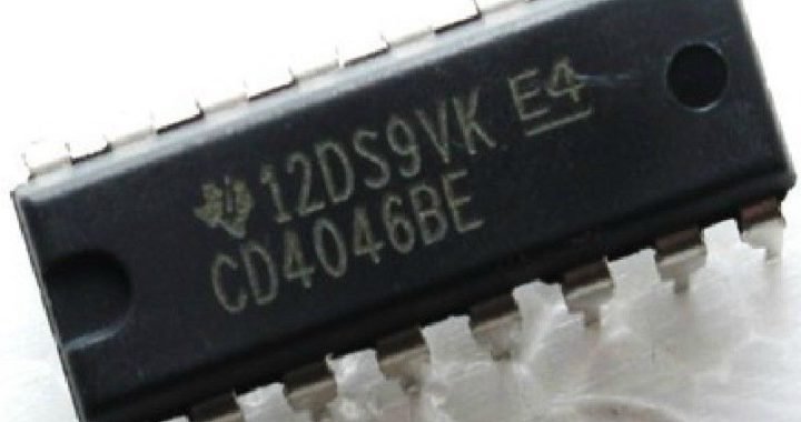
CD4046 SPICE model

The CD4046 is an electronic component that belongs to the family of CMOS integrated circuits (Complementary Metal-Oxide-Semiconductor). It is a PLL (Phase-Locked Loop), which is a feedback control system with the capability to synchronize the phase of an output signal with that of a reference input signal. This component is primarily used in analog and digital electronic applications to generate, demodulate, synchronize, and modulate signals. After a brief overview of the component, the CD4046 SPICE model will be presented, offering comprehensive insights into its behavior and characteristics.

The CD4046 is primarily composed of three fundamental parts:

  1. VCO (Voltage-Controlled Oscillator): This section generates an oscillating signal whose frequency is controlled by the control voltage. The output frequency is directly proportional to the input voltage, making it useful for generating variable-frequency signals.
  2. Phase Detector: This part of the circuit compares the phase of the input signal with that of the feedback signal from the VCO output. Any phase difference between these two signals generates an error signal used to adjust the VCO frequency, ensuring that the phase of the output signal aligns with that of the input signal.
  3. Divider: This section includes division circuits that can be used to divide the frequency of the input signal or the feedback signal. This division can be useful for achieving desired frequency ratios in the synchronization process.

The main uses of the CD4046 include:

Frequency Demodulation:

The CD4046 can be used to demodulate frequency-modulated (FM) signals by converting them into voltage signals. This is useful in applications such as receiving FM radio signals.

Variable-Frequency Signal Generation:

Thanks to the VCO, the CD4046 can generate output signals with a variable frequency controlled by a voltage. This is useful in musical synthesizers, testing instruments, and other applications where generating variable-frequency signals is necessary.

Phase Detection:

The CD4046 can be used to detect phase differences between two signals. This is valuable in electronic control systems, optical alignment systems, and other applications where phase synchronization is important.

Frequency Tracking:

It can be used to monitor frequency variations in an input signal and generate an output signal proportional to these variations. This can be beneficial in frequency control applications.

Now let’s take a look at the CD4046 SPICE model:

.subckt CD4046 sigin phcmpii phcmpi phpls compin vcoin
+              r1 r2 ce1 ce2 vcoout demout inhibit zener vdd vss
+                   OPTIONAL: DPWR=$G_DPWR DGND=$G_DGND
+                   PARAMS: MNTYMXDLY=0 IO_LEVEL=0
+                   Rin=1Meg S1=1  S2=0.5 M1=0.5 M2=1.0 Vx=10
+                   Kb=1 Vfree=0.0 Kc=-0.1 Vt=1.2 Vxqr=10

* Rin  = VCO Input Resistace
* S1   = Voltage Limiter linear slope
* S2   = Voltage Limiter non-linear slope
* Vx   = Input threshold voltage (between S1 and S2)
* Kb   = Arbitrary constant to adjust the value of the conversion gain (transimpedance gain)
* Vfree= Frequency dependent constant in Emult
* Kc   = Negative inverse amplitude of the square wave
* Vt   = Trigger voltage of Schmitt trigger (not used)
* Vxqr = Amplitude of square wave (not used)
* M1   = Current mirror multiplier to adjust oscillator frequency
* M2   = Current mirror multiplier to adjust oscillator frequency

*The provided portion of the CD4046 SPICE model defines a subcircuit with the following parameters:

* r1, r2, ce1, ce2, vcoout, demout, inhibit, zener, vdd, vss are the subcircuit component nodes.

*Optional parameters are DPWR and DGND.

*Parameters are set with values: MNTYMXDLY=0, IO_LEVEL=0, Rin=1Meg, S1=1, S2=0.5, M1=0.5, M2=1.0, *Vx=10, Kb=1, Vfree=0.0, Kc=-0.1, Vt=1.2, Vxqr=10.

* Preliminary model still under development based on Natinal Semiconductor CD4046BM
* RAPerez 9/98

* Phase detector section

U1 INVA(4) DPWR DGND sigin compin isigin icompin
+                    isigin icompin clk1 clk2
+ INVA_TIMING IO_HCT
+ MNTYMXDLY={MNTYMXDLY} IO_LEVEL={IO_LEVEL}

.MODEL INVA_TIMING UGATE

U2 XOR DPWR DGND isigin icompin xorout
+ XOR_TIMING IO_HCT
+ MNTYMXDLY={MNTYMXDLY} IO_LEVEL={IO_LEVEL}

.MODEL XOR_TIMING UGATE
***tplhty=20n tphlty=20n

U3 NAND(2) DPWR DGND q1 q2 pclr
+ NAND_TIMING IO_HCT
+ MNTYMXDLY={MNTYMXDLY} IO_LEVEL={IO_LEVEL}

.MODEL NAND_TIMING UGATE (tplhty=1n tphlty=1n)

U4 DFF(1) DPWR DGND $D_HI clr clk1 $D_HI q1 qb1
+ DFF1_TIMING IO_HCT
+ MNTYMXDLY={MNTYMXDLY} IO_LEVEL={IO_LEVEL}

.MODEL DFF1_TIMING UEFF tppcqlhty=4n tppcqhlty=4n tpclkqlhty=4n tpclkqhlty=4n

U5 DFF(1) DPWR DGND $D_HI clr clk2 $D_HI q2 qb2
+ DFF2_TIMING IO_HCT
+ MNTYMXDLY={MNTYMXDLY} IO_LEVEL={IO_LEVEL}

.MODEL DFF2_TIMING UEFF tppcqlhty=5n tppcqhlty=5n tpclkqlhty=5n tpclkqhlty=5n

U7 BUFA(2) DPWR DGND fq1 fq2 s1 s2
+ BUFA_TIMING IO_HCT
+ MNTYMXDLY={MNTYMXDLY} IO_LEVEL={IO_LEVEL}

.MODEL BUFA_TIMING UGATE

ST2 vdd phcmpii s1 0 swt
SB2 phcmpii vss s2 0 swt

.model swt VSWITCH (ROFF=2G RON=10m VOFF=0.8 VON=3.0)

U6 AND(2) DPWR DGND pclr reset clr
+ AND_TIMING IO_HCT
+ MNTYMXDLY={MNTYMXDLY} IO_LEVEL={IO_LEVEL}

.MODEL AND_TIMING UGATE

Ureset STIM(1,1) DPWR DGND
+ reset
+ IO_HCT
+   +0s 0
+   2ns 1
+   1s 1

U8 NOR(2) DPWR DGND fq1 fq2 norout
+ NOR_TIMING IO_HCT
+ MNTYMXDLY={MNTYMXDLY} IO_LEVEL={IO_LEVEL}

.MODEL NOR_TIMING UGATE

U9 ANDA(2,2) DPWR DGND q1 od1 q2 od2 fq1 fq2
+ ANDA_TIMING IO_HCT
+ MNTYMXDLY={MNTYMXDLY} IO_LEVEL={IO_LEVEL}

.MODEL ANDA_TIMING UGATE

U10 DLYLINE DPWR DGND q1 od1
+ DLY_TIMING IO_HCT
+ MNTYMXDLY={MNTYMXDLY} IO_LEVEL={IO_LEVEL}
U11 DLYLINE DPWR DGND q2 od2
+ DLY_TIMING IO_HCT
+ MNTYMXDLY={MNTYMXDLY} IO_LEVEL={IO_LEVEL}

.MODEL DLY_TIMING UDLY dlyty=12n

U12 BUFA(3) DPWR DGND norout xorout vcosqr phpls phcmpi vcoout
+ BUFB_TIMING IO_HCT
+ MNTYMXDLY={MNTYMXDLY} IO_LEVEL={IO_LEVEL}

.MODEL BUFB_TIMING UGATE

* The above portion of CD4046 SPICE model represents various sections of the circuitry within the component:

*Phase Detector Section: This section encompasses multiple subcircuits and models to simulate the behavior of the phase detector *and related components. These include logic gates like NAND, XOR, D-type flip-flops, AND, BUFA, ANDA, DLYLINE, and BUFB. *Each subcircuit is configured with specific timings and parameters for accurate simulation.

*Logic Gates: Different logic gates are utilized to implement the functionality of the phase detector. These gates include NAND, *XOR, AND, BUFA, ANDA, etc., each having their specific timing and connectivity configurations.

*Switch Model: The model “swt” represents a voltage-controlled switch. It’s used to simulate the switching behavior in the circuit.

*Stimulus Source: A stimulus source named “Ureset” generates a reset signal for simulation purposes. It provides an initial value of *0, switches to 1 after 2 nanoseconds, and maintains 1 from that point onward.

*Timing Models: Various subcircuits (NAND_TIMING, DFF1_TIMING, DFF2_TIMING, BUFA_TIMING, etc.) are configured with *specific timing parameters to accurately replicate the behavior of the corresponding logic components.

*Model Parameters: The models are configured with parameters such as “MNTYMXDLY” and “IO_LEVEL” to adjust the simulation *behavior as needed.

* VCO Section

Rin vcoin vss {Rin}
Evlim vlim 0 value={if(v(vcoin,vss)<v(vdd,vss),
+                   S1*v(vcoin,vss),S2*(v(vcoin,vss)-v(vdd,vss))+v(vdd,vss))}
Rvlim vlim 0 1Meg
Emult mix 0 value={v(vlim)*Kb+Vfree}
*Hmult mix 0 poly(1) Vcm 1.44 0.586
Rmult mix 0 1

Edemout demout 0 table={ 200Meg*v(vcoin,demout)*v(off) } (-20,-20) (20,20)
Rdemout demout 0 1Meg
ER2 ir2 0 vdd ir2 200Meg
VR2 ir2 r2
ER1 ir1 0 mix ir1 200Meg
VR1 ir1 r1
Eosclg adj 0 table={abs((V(vdd)/I(VR2))/(V(mix)/I(VR1)))}
+ (0.5,1.43) (1,1.6) (10,1.04) (50,0.67) (100,0.84) (101,1)
+ (102,1) (1000,1)
Radj adj 0 1G
*GIM ce1 0 value={(M1*I(VR1)+M2*I(VR2))*Kc*V(sqrrc)}
GIM ce1 0 value={(M1*I(VR1)*V(adj)+M2*I(VR2))*Kc*V(sqrrc)}
*GIM ce1 0 value={(24*I(VR1)+3.067*I(VR2))}
Vcext ce2 0
Cstray ce1 ce2 6p
Rcext ce1 ce2 1T
Etrngl trngl 0 ce1 0 1
Rtrngl trngl 0 1Meg

Esqr sqr 0 value={-10Meg*V(trngl)+1.2Meg*V(sqrrc)}

Rsqr sqr sqrrc 0.1T
Csqr sqrrc 0 10f
Dsqr1 sqrrc 13 Diode
Vsqr1 13 0 {Vx}
Dsqr2 14 sqrrc Diode
.model Diode D (IS=10u N=0.1 CJO=80f RS=1m)
*.model Diode D (IS=10u N=0.001 CJO=80f)
Vsqr2 14 0 {-Vx}
Ipls 0 sqrrc pwl 0 0 10n 0 20n 0.01u 0.1u 0.01u 0.12u 0 1 0
Evcoout vcosqr 0 table={5.0*v(off)*(v(sqrrc)/Vx)} (0.1,0.1) (4.5,4.5)
*Rvcoout vcosqr vcosqr1 1

**Et 7 0 TABLE {-10k*V(trngl)+1.2k*V(sqrrc)} (-2,-10) (2,10)
*Ipls 0 sqrrc pwl 0 0 10n 0 20n 1u 0.1u 1u 0.12u 0 1 0
*Et 7 0 value={table({-10Meg*V(trngl)+1.2Meg*V(sqrrc)},-10,{-Vx},10,{Vx})}
*Ro 7 sqrrc 100
*Co sqrrc 0 100p

*Est sqrrc o VALUE={table({2000k*(V(st)-V(trngl))},-2,{-Vx},2,{Vx})}
*Rst1 sqrrc st 8.8k
*Rst2 st 0 1.2k
*Cst st 0 200p ic=-10

Rinhbt inhibit 0 1Meg
Eoff off 0 value={if(v(inhibit)<0.9,1.0,0.0)}
Roff off 0 1Meg

Dzener vss zener znr
Rzener vss zener 1G
.model znr D(Is=1.004f Rs=.5875 Ikf=0 N=1 Xti=3 Eg=1.11 Cjo=160p M=.5484
+  Vj=.75 Fc=.5 Isr=1.8n Nr=2 Bv=5.2 Ibv=27.721m Nbv=1.1779
+  Ibvl=1.1646m Nbvl=21.894 Tbv1=176.47u)

.ends

This portion of the CD4046 SPICE model describes the “VCO Section” of the circuit. It includes various components and their connections that are responsible for controlling the Voltage-Controlled Oscillator (VCO) behavior within the CD4046:

  • Rin and vcoin are connected to set the VCO input resistance.
  • The section involving Evlim calculates the voltage limit for the VCO input signal based on specified conditions.
  • Rvlim defines the resistance for voltage limiting.
  • Emult calculates the multiplication of the voltage limit and a constant, along with Rmult representing resistance for multiplication.
  • Edemout and Rdemout define components for generating the demodulated output signal.
  • Eosclg calculates a frequency dependent constant, utilizing the adjacent voltage.
  • Various components like Radj, GIM, Vcext, Cstray, Rcext, Etrngl, Rtrngl, Esqr, Rsqr, Csqr, Dsqr1, Vsqr1, Dsqr2, Vsqr2 further shape and process the VCO output signal.
  • Ipls generates a piece-wise linear current source.
  • Evcoout calculates the voltage of the VCO output signal.
  • The section involving Dzener and Rzener defines a diode and resistor for zener voltage regulation.
  • The .model znr part provides model parameters for the zener diode.

This portion of the SPICE model focuses on the detailed components and connections that constitute the VCO section of the CD4046, enabling simulation and analysis of its behavior in various scenarios.

You can find the datasheet of this component available for download Here.

Circuit Breaker SPICE Simulation.

Experience precise Circuit Breaker SPICE Simulation with an advanced electrical model. Accurately replicate behavior across overcurrents, including the magnetic region. Validated against real-world tests, enhance protection performance in telecom DC systems.


T. ROBBINS
TELSTRA RESEARCH LABORATORIES
BOX 249 ROSEBANK MDC, CLAYTON VICTORIA 3168, AUSTRALIA
Email: t.robbins@trl.oz.au

Abstract: This article describes an electrical model of a thermalmagnetic circuit-breaker that can accurately simulate characteristic behaviour over a wide range of overcurrents, including operation in the magnetic region. The model has been validated against measured waveforms from both a high-current DC test facility and a distributed power system rack. The circuit-breaker model can be coupled with other distribution component models to simulate the protection performance in telecommunications DC distribution systems.

1.Introduction

The design and analysis of over-current protection for telecommunication DC power systems can be greatly assisted by the use of a computer-aided simulation tool. However, a simulation is only as accurate as the component models and element values used to represent the real world. This article reports on the development of a circuit-breaker model that can accurately represent circuit-breaker behaviour over a wide range of overcurrents.

The performance of protection, distribution and storage devices significantly affects both the reliability and safety of the DC power system. Voltage excursions caused by an over-current instance can cause electronic equipment to malfunction due to over-voltage, and disrupt service due to under-voltage. Poor discrimination between protection devices can cause upstream device operation, resulting in major interruption to service. The rapid advancement of both computing power and analogue circuit simulation programs derived from SPICE software provides a relatively user-friendly environment for over-current protection design and analysis. This is advantageous as telecommunications power distribution systems are often large and complex, and developing an equivalent circuit model for a power system is not a trivial task.

The circuit-breaker model described in this article implements the enhanced modelling functions available with PSpice’s Analog Behavioural Modelling to include circuit-breaker current, time and arcing dependent characteristics. This model complements and extends previously published modelling work [1-2] by Telstra Research Laboratories on other power system components.

2.Circuit-Breaker Characteristic Operation

A typical thermal-magnetic circuit-breaker operates (trips) in two distinct modes; the thermal mode occurs for device currents from 1 up to about 10-15 times the rated setting current, and the magnetic mode occurs for all current levels above the thermal operating region. Characteristic current-time curves for the device operating in the thermal region can be approximated by an equation where i n t equals a constant, whereas in the magnetic region the operating time (typically <20ms) is not well defined in device data curves and specifications, as test circuits are based on rectified AC power sources which have typical rise times exceeding a few milliseconds.

The circuit-breaker model presented in this paper has been developed for a 125A moulded device (10kA fault rating), which is commonly used to protect individual battery strings within Telstra’s distributed power supplies.

For device operation in the thermal region, the characteristic i n t form of the current-time curve can be obtained from the device specification curve as shown in Figure 1. A value of n = 3.5 gives an adequate fit over the range of currents within the thermal operating region.

Fig.1 125A circuit-breaker current-time operating boundary curves (courtesy of GEC ALSTHOM AUSTRALIA).
Fig.1 125A circuit-breaker current-time operating
boundary curves (courtesy of GEC ALSTHOM
AUSTRALIA).

For device operation in the magnetic region, characteristic current-arc voltage-time behaviour has been observed for the circuit-breakers operating in a high-current DC test facility over a range of current levels and circuit time constants. At the start of such a fault instance, the current passing through the closed circuit-breaker contacts increases to a level where magnetic activation forces the contacts to open. As the contacts start to open an arc is developed which is inherently unstable and a complex voltage-current characteristic occurs as the arc progresses through to extinction.
For the 125A circuit-breaker operating in the magnetic region, the contacts are forced open when the current level typically rises above 2-4kA. Circuit-breaker operation was measured over a range of circuit conditions, such as:

· fast rates of current rise exceeding 10kA/ms, which resulted in short pre-arcing times of about 0.15- 0.2ms (eg. results from a test circuit with 5.4kA prospective current and 0.26ms time constant are shown in Figure 2).

· high prospective current levels exceeding 10kA, which result in pre-arcing times around 0.9ms for circuit time constants of about 1.2ms, as shown in Figure 3. It should be noted that special oscilloscope probing and current shunt techniques are required to record clean waveforms in the high transient noise environment that occurs in a high current test facility.

Fig.2 Measured current and voltage waveforms for a 125A circuit-breaker operating in 54VDC test circuit with 5.2kA prospective current and 0.25ms prospective time constant; 1kA/div current, 20V/div voltage and 0.5ms/div.
Fig.2 Measured current and voltage waveforms for
a 125A circuit-breaker operating in 54VDC test circuit
with 5.2kA prospective current and 0.25ms prospective
time constant; 1kA/div current, 20V/div voltage and
0.5ms/div.
Fig. 3 Measured current and voltage waveforms for a 125A circuit-breaker operating in 54VDC test circuit with about 12kA prospective current and about 1ms prospective time constant; 1kA/div current, 50V/div voltage and 0.5ms/div.
Fig. 3 Measured current and voltage waveforms for
a 125A circuit-breaker operating in 54VDC test circuit
with about 12kA prospective current and about 1ms
prospective time constant; 1kA/div current, 50V/div
voltage and 0.5ms/div.

Fuse Model SPICE Simulation.

Fuse Model SPICE Simulation. The creation of a precise fuse model within SPICE-derived software. Discover how this model accurately captures characteristic fuse parameters and can even be tailored to simulate circuit breaker operations. Streamline your over-current protection design for telecommunication DC power systems with cutting-edge simulation tools.


T. Robbins
Telecom Australia Research Laboratories
770 Blackburn Road, Clayton, 3168
Australia

Abstract: The design and analysis of over-current protection for telecommunication DC power systems can be greatly assisted by the use of a computer-aided simulation tool. This article reports on the development of a fuse model for SPICE derived software that can accurately represent characteristic fuse parameters. The fuse model can also be adapted to represent the operation of circuit breakers.

1.Introduction

The design and analysis of over-current protection for telecommunication DC power systems can be greatly assisted by the use of a computer-aided simulation tool. However, a simulation is only as accurate as the component models and element values used to represent the real world. This article reports on the development of a fuse model that can accurately represent fuse characteristics. The fuse model can also be adapted to represent the operation of circuit breakers.
The performance of over-current protection devices significantly affects both the reliability and safety of the DC power system. Voltage excursions resulting from the operation of a fuse during a short circuit can cause electronic equipment malfunction due to over-voltage, and disrupt service due to under-voltage. Poor discrimination between protection devices can cause upstream device operation, resulting in major interruption to service.

The rapid advancement of both computing power and analogue circuit simulation programs derived from SPICE software provide a user-friendly environment for over-current protection design and analysis. This environment is advantageous as telecommunications power distribution systems are often large and complex, and developing an equivalent circuit model for apower system is not a trivial task.

The analysis of DC distribution systems using computer simulation has been shown to provide fair agreement between simulated and experimental results [1,2,3]. However, the fuse models developed have not been able to accurately represent fuse characteristics. Typical parameters for a fuse operating in a circuit with a given time constant and prospective current are rated current ir, peak current ip, pre-arcing time tp, arcing time ta, total operating time tt= tp + ta, pre-arcing i²t (i²t)p, arcing i²t (i²t)a and total operating i²t (i²t)t= (i²t)p + (i²t)a. Figure 1 illustrates some of these parameters. The prospective current for a circuit is the maximum current that would be reached if the fuse did not operate.

The i²t or current-squared time rating is a commonly used fuse characteristic when operating current levels are much higher that the rated fuse current ir. The circuit time constant defines the ratio L/R, where L and R are the effective circuit inductance and resistance components in series with the fuse and energy source.

Typycal fuse parameters
Fig 1. Typycal fuse parameters

A fuse model is developed in Section 2 and model validation is undertaken in Section 3. Section 4 discusses the development of other DC power system component models for application to the analysis of over-current protection, and the paper is summarised in Section 5.

Combination Wave Generator SPICE simulation.

In this article, we will delve into the implementation and analysis of a versatile Combination Wave Generator SPICE simulation template. This template forms the groundwork for a range of applications including Surge Generators, Line Impedance Stabilization Networks (LISN), motor control, and ripple current analysis. Hardware engineers can capitalize on this model to streamline project development efforts.While using PSpice for simulation, you can effortlessly apply the fundamental principles of the Combination Wave Generator SPICE simulation template to various other SPICE simulation software platforms.

A “Combination Wave Generator” finds its application in Electromagnetic Compatibility (EMC) tests, generating specific waveform voltage or current pulses. Its purpose is to assess electronic devices’ electrical resilience and responses to abrupt variations or transients within the electromagnetic environment. These generators replicate transient electrical disruptions or surges that might manifest in electronic circuits during situations like electrostatic discharges, switching transients, or line surges.

The Combination Wave Generator is an essential component of EMC compliance tests, ensuring that electronic devices can operate in realistic electromagnetic environments without sustaining damage or unforeseen behaviors.

Simplified SPICE Model of Combo Wave Generator.

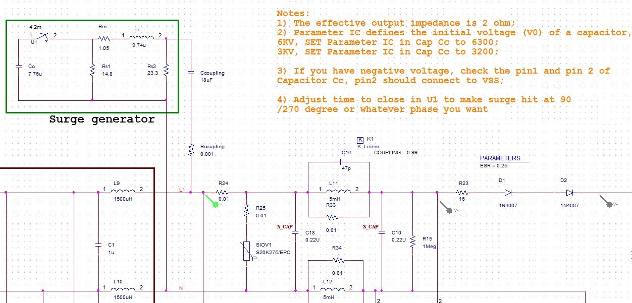
The simplified model of the CWG consists of an High-Voltage source U, a charging resistor Rc, an energy storage capacitor Cc. This part of circuit is connected by a switch to 2 Pulse duration shaping resistors Rs, an impedance matching resistor Rm and a Rise time shaping indutor Lr, as in the picture below


GPM-SurgeGenerator_page3_image1


typical values of this components are:  Cc=7.76μF,  Rs1=14.8 Ohm,  Rm=1.05 Ohm,  Lr=9.74μH,  Rs2=23.3 Ohm. The peak voltage on Rs2 can be 1KV, 2KV,..6KV.

In the following schematic we set the high voltage with the initial condition of the CapacitorCc, for example for 6KV, we set 6300 in the PSpice IC field of the Cc component. We can adjust the time in U1 to make surge hit at 90/270 degree or whatever phase we want.


GPM-SurgeGenerator_page4_image1
GPM-SurgeGenerator_page4_image2


Calibration of Surge Generator.

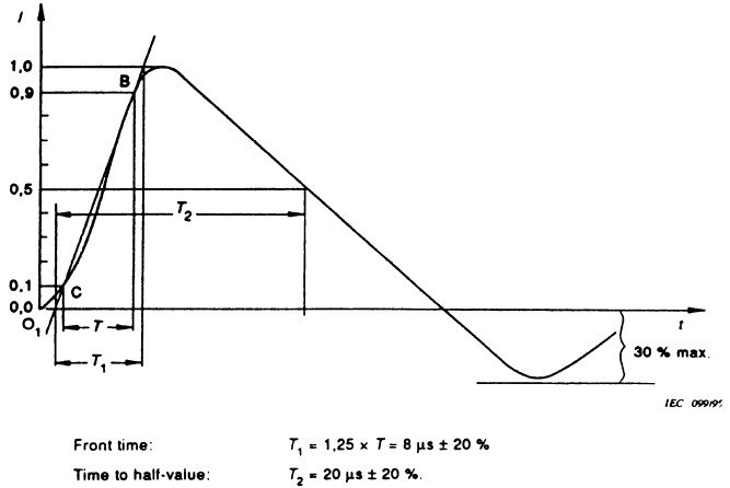
The IEC/EN 61000-4-5 standars requires the following waveform of open-circuit voltage with no Coupling/Decoupling network (CDN) connected


GPM-SurgeGenerator_page5_image1


This is the result of the simulation that shows a voltage waveform that fullfills requirementof IEC/EN 61000-4-5

GPM-SurgeGenerator_page5_image2


Below the image of the waveform of short-circuit current with no CDN connected

GPM-SurgeGenerator_page6_image2


and here again the simulated results:


GPM-SurgeGenerator_page6_image1


Ipeak is about 1.5KA, T1 is 8uS and T2 is 20uS. The effective coupling impedance is 2Ohm. The simulated current waveform fulfills requirement of IEC/EN 61000-4-5 standards.

OrCAD PSpice Video Tutorials

TopicVideo
Getting started with OrCAD Capture
OrCAD PSpice how to perform a Bias point analysis 1
OrCAD PSpice how to perform a Bias point analysis 2
OrCAD PSpice, how to perform a transient analysis
How to mark Voltage and Currents in OrCAD PSpice
How to perform a DC Sweep Analysis in PSpice OrCAD
Performing an AC Sweep Analysis in PSpice OrCAD
Using the Monte Carlo Analysis in PSpice OrCAD
Worst-Case Circuit Analysis with PSpice
A Differential Amplifier Analyzed with PSpice
How to design the current source for a Differential Amplifier with PSpice
A complete video tutorial from the schematic to the PCB layout with OrCAD PCB Editor

SPICE modeling of Magnetic Core from Datasheet

Vittorio Carboni

Department of Electronics and Automatic, University of Ancona 1999/2000

SPICE simulations and analisys by Ing. Cristoforo Baldoni

1. Switching  power supply: Choice of ferrite

2. Simplified calculation of the transformer

3. Transformer for Flyback converter: Calculation example

4. Transformer for Forward converter :Calculation example

5. Windings: Supports, wires and insulation


On what

How

With what

Skin and proximity effects

6. Let’ s complete the design of the flyback transformer

Primary

Secondary

Conclusions

7. Appendix

8. SPICE modeling of ETD49 N67 core from datasheet

9. Bibliography


1. Switching  power supply: Choice of ferrite

The first step in the design of the transformer is the choice of the ferrite as physical form,  type of material and dimensions. It’s a very important choice that characterizes the project as all subsequent calculations based on it. An error of assessment may lead, at the end of designing, to realize, for example, that the dimensions are not suitable: this means start again with considerable lost of time and resources.

The ferrites are characterized by very low losses at high frequencies, they are made with alloys of iron oxides and other metals such as zinc and manganese. The material is pulverized together with insulating oxides and then modeled using techniques typical of ceramics. This allows to make ferrites with a great variety of shapes and sizes and tolerances very restricted about magnetic and mechanically characteristics. They, also, can be machined with precision after the operation of the cooking.

The ferrites typically have a density of the saturation flux between 3 and 5 kGauss, also the presence of oxides increases its specific resistivity at very high levels thus allowing to reduce losses due to eddy currents. The available shapes include bars, toroids, EE EI and UI cores. The Curie temperature TC, namely the temperature at which the material loses its ferromagnetic properties, is between 100 and 300 ° C, depending on the type of material; the phenomenon is reversible, reducing the temperature to below the TC material regains its properties.

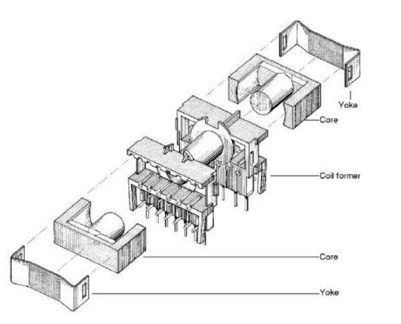
For low to medium power transformers E-Series is the best choice. As the acronym suggests, the magnetic core is composed of two elements in the shape of E. The two pieces forming the magnetic circuit, are slipped into the holder of the windings and locked in place with the clips and / or bonded with Araldite or other epoxy adhesives. The three contact surfaces of the half-cores are machined so as to reduce the roughness and therefore contain to negligible size the not intentional air gap . In some cases the air gap is desired, this can be obtained realizing the central column of the half-core shorter than outer ones.

figure1

Figure 1 – Example of assembling of a kit composed of the support for the windings, a pair of ferrites of ETD type and a pair of fastening clips. (FERRITES and Accessories, Siemens Matsushita Components)

It’s possible choose from a catalog of half-cores with air gap calibrated. For the ferrite type ETD49, for example, we can have 4 values of the air gap: 0.20 +- 0.02 mm, 0.50 +- 0.05 mm, 1.00 +- 0.05, 2.00 +- 0.05 mm.

Coupling a half-core with air gap with another without, or also with air gap, also of different value, it is possible to obtain numerous combinations.

The ferrites of series E and ETD are widely used, so are easy to find. The catalog Siemens Matsushita indicates that the materials available for the E-series are different and coded with the initials N27, N67, N87, N49, N30, T37. The choice of material to use is correlated with the switching frequency: the type N27 is suitable for power applications in a frequency band of switching up to 100KHz, N67 is suitable for similar application, but the frequency range is between 100KHz and the 300KHz. Table 1 shows the possible applications for different materials. The E series has the classical central square column, other families in the same series are available for special applications such as the best known:

ETD stands for Economic Transformer Design, with circular cross-section of the center column

EFD stands for Economic Flat Design transformer for applications with space vertical content.

table1

Table 1 – Some parameters for the type ferrites ETD (FERRITES and Accessories, Siemens Matsushita Components).

Table 2 – Maximum permissible temperature rise for different materials (FERRITES and Accessories, Siemens Matsushita Components).

Table 3 – Thermal resistance for different types and sizes of ferrite (FERRITES and Accessories, Siemens Matsushita Components).

The most important parameters for a correct choice of the ferrite are:

1. Maximum power (Ptrans)

2. Type of converter (Forward, Flyback, Push-Pull)

3. Switching frequency and maximum permissible temperature

4. maximum volume

To make the choice you might consider that the manufacturer, as a rule, always indicates the limit values, so if it is not pressing the issue of costs, it is a good idea to choose on the table, the type immediately above the one that delivers the requested power. This will avoid,later in the phase of winding, to discover that the number of turns calculated, with the wire section calculated does not enter for lack of space in the throat of the support of the windings. This precaution is especially recommended if the transformer should be wrapped in accordance with the safety standards (minimum distances between the different layers of the windings, using wire with double insulation etc..).

It follows an example of calculation of a switching transformer in [1]; the approach to this type of  calculation is in many passages forcibly empirical, in many other simplified. On the other hand a completely theoretical discussion would result in a significant waste of resources without the benefits of improved performance.

SPICE modeling of a JFET from Datasheet

In this article we’ ll see how to find the parameters used to describe the mathematical behaviour of JFET (Junction Field Effect Transistors).The syntax for the N-channel model is:

model ModelName NJF( par1=a par2=b………parn=x)

while for the P-channel model is:

model ModelName PJF( par1=a par2=b………parn=x)

Where par1 par2… parn are the parameters that allow us to model the equations of the JFET transistor.

The main parameters for modeling the JFET are listed below in this table:


ParametersDescriptionUnitsDefault Value
AFFlicker noise exponentno unit dimension1.0
ALPHAIonization coefficient1/V1e-006
BETATransconductance coefficientA/V^20.0001
BETATCEBETA exponential temperature coefficient%/°C-0.5
CGDZero-bias gate-drain p-n capacitanceF1e-012
CGSZero-bias gate-source p-n capacitanceF1e-012
FCForward-bias depletion capacitance coefficientno unit dimension0.5
ISGate p-n saturation currentA1e-014
ISRGate p-n recombination current parameterA0
KFFlicker noise coefficientno unit dimension1e-018
LAMBDAChannel-length modulation1/V1e-006
MGate p-n grading coefficientno unit dimension0.5
NGate p-n emission coefficientno unit dimension1.0
NREmission coefficient for ISRno unit dimension2.0
PBGate p-n potentialV1.0
RDDrain ohmic resistanceOhm1.0
RSSource ohmic resistanceOhm1.0
VKIonization knee voltageV1.0
VTOThresold voltageV-2.0
VTOTCVTO temperature coefficientV/°C-0.0025
XTIIS temperature coefficientno unit dimension3.0

SPICE modeling of a BJT from Datasheet

BJT bipolar transistors require a certain number of parameters to get a good model.The syntax for this model is:

.model ModelNameNPN (par1=a par2=b………parn=x)

for PNP case:

.model ModelNamePNP (par1=a par2=b………parn=x)

where par1 par2…….parn are the parameters that allow to model equations of the BJT.

The main parameters for a reasonable modeling of the behavior of the component are summarized in the following table:

ParametersDescriptionUnitsDefault Value
ISTransport saturation currentA1e-16
XTIIS temperature effect exponentno unit dimension3.0
EGBandgap voltage (barrier height)eV1.11
VAFForward Early voltageVInfinite
BFIdeal maximum forward betano unit dimension100
ISEBase-emitter leakage saturation currentA0
NEBase-emitter leakage emission coefficientno unit dimension1.5
IKFCorner for forward-beta high-current roll-offAInfinite
NKHigh-current roll-off coefficientno unit dimension0.5
XTBForward and reverse beta temperature coefficientno unit dimension0
BRIdeal maximum reverse betano unit dimension1.0
ISCBase-collector leakage saturation currentA0
NCBase-collector leakage emission coefficientno unit dimension2.0
IKRCorner for reverse-beta high-current roll-offAInfinite
RCCollector ohmic resistanceOhm0
CJCBase-collector zero-bias p-n capacitanceF0
MJCBase-collector p-n grading factorno unit dimension0.33
VJCV0.75
FCForward-bias depletion capacitor coefficientno unit dimension0.5
CJEBase-emitter zero-bias p-n capacitanceF0
MJEBase-emitter p-n grading factorno unit dimension0.33
VJEBase-emitter built-in potentialV0.75
TRIdeal reverse transit timesec1e-8
TFIdeal forward transit timesec0
ITFTransit time dependency on IcA0
XTFTransit time bias dependence coefficientno unit dimension0
VTFTransit time dependency on VbcVInfinite
RBZero-bias (maximum) base resistanceOhm0

SPICE modeling of a Diode from Datasheet

Modeling in SPICE& a diode is not a trivial work. Although the operation of the diode is quite simple, extract a model from datasheet takes some time.Every component has its own syntax defined in SPICE , in the case of the diode:

.model ModelName D (par1=a par2=b………parn=x)

where par1 par2 …. parn are characteristic parameters of diode.

we can sum up the set of main parameters in the following table:

ParameterDescriptionUnitDefault value
BVReverse breakdown knee voltageVInfinite
CJOZero-bias p-n capacitanceF0
EGBandgap voltageeV1.11
FCForward-bias depletion capacitance coefficientno unit dimension0.5
IBLVLow-level reverse breakdown knee correntA0
IBVReverse breakdown knee correntA1e-10
IKFHigh-injection knee currentAInfinite
ISSaturation correntA1e-14
ISRRecombination current parameterA0
Mp-n grading coefficientno unit dimension0.5
NEmission coefficientno unit dimension1.0
NREmission coefficient for ISRno unit dimension2.0
RSParasitic resistanceOhm0
TTTransit timesec0
VJp-n potentialV1.0
XTIIS temperature exponentno unit dimension3.0

All these parameters are used by SPICE to describe the behavior of the diode in the different situations of signal, for example in direct polarization in DC that, forward current will be:

ID = IS*(e^(VD/(N*Vt))-1)

where VD is the forward voltage, Vt = k * T / q is the thermal voltage equal to 0.026 V at 27 degrees Celsius.

The so-called recombination current is instead calculated as

Irec = ISR*(e^(VD/(N*Vt))-1).

Other equations from the given parameters describing the capacitance of the junction, its evolution with temperature and more.

At this point we have to derive the various parameters from the datasheet of the component. Assume we want to model a silicon diode 1N4148. The extraction of the parameters of the table from the values reported in the datasheet, is not immediate for almost none of the parameters.look at the values of our interest in datasheet:

data1

From the table we can get BV which is equal to VRM, in other cases reported as Vbr, or in the case of Zener diode Vz.

data2

From this second table we see that the maximum leakage current at 25 degrees is Ir = 5 uA.We can take IBV as equal to 10 times Ir. Usually for this type of diodes the value of IBV is around 100uA. For Zener diodes Ir can be called Izk, or in other cases as Ibr.

CJO can be directly equal to the value specified in the datasheet as Cj or Ctot, in this case is 4pF.