ChatGPT-Assisted BJT SPICE Modeling: Complete Workflow from Datasheet to Simulation
Learn how to generate a SPICE model of the 2N2222 transistor using ChatGPT. Step-by-step AI prompts, parameter extraction, and model validation with SPICE simulations under typical operating conditions.
The article “SPICE Modeling with AI: Powering Electronic Device Modeling” explains in its section on AI-driven model generation and optimization that artificial intelligence can automatically create SPICE models directly from device datasheets. In this tutorial, we will develop that same technique step by step, using different AI models to assist in building a SPICE representation of a 2N2222 NPN transistor, one of the most common and well-documented small-signal BJTs.
The 2N2222A is an ideal example device because its datasheets are rich in numerical tables, characteristic curves, switching diagrams, and capacitance plots — all essential elements for accurate SPICE parameter extraction. The goal of this tutorial is not merely to reproduce a specific transistor model, but to demonstrate a general workflow that can be applied to any BJT.
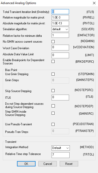
The models produced throughout this process should be regarded as representative of typical operating conditions, generally accurate within a few percentage points depending on the quality of the datasheet and the AI model used. However, as with all simulation models, verification is essential. Each generated SPICE file should be validated using appropriate testbenches, DC/AC/transient simulations, sensitivity analysis, or corner explorations to confirm its practical reliability.
The first step in this process is to obtain a complete and detailed datasheet for the target device. This includes not only the electrical characteristic tables but also as many graphical plots as possible — transfer curves, output characteristics, capacitance–voltage graphs, and switching performance diagrams. These figures provide the quantitative foundation that AI models use to interpret the device and build accurate SPICE parameters.
Once the datasheet is ready, we can construct a structured AI prompt to guide ChatGPT in the data extraction and model generation phases. A well-designed prompt ensures that numerical values, curve trends, and device behaviors are correctly interpreted and translated into a SPICE-compatible format. This greatly increases the reliability and efficiency of AI-assisted model generation.
In the following section, we will prepare the complete prompt used to generate the SPICE model for the 2N2222A.
You can copy and paste this prompt directly into ChatGPT (preferably GPT-5), attach the device datasheet, and let the AI extract, interpret, and assemble the transistor model automatically.
PROMPT Structure for BJT SPICE Modeling:
Role and Modeling Objectives
You are an expert electronic device modeler and SPICE engineer.
Given one or more PDF datasheets (and optional measurement or characterization files), your task is to analyze, extract, derive, and validate all electrical parameters needed to build a complete, physics-based, and PSpice-compatible SPICE model using SPICE3 syntax.
All parameters must be supported by datasheet evidence, measured data, or physically justified derivations.
Never assume or interpolate values silently. Each parameter must include a source, method, and confidence level.
Required Datasheet Inputs for the Prompt
- Required: Main datasheet PDF(s).
- Optional: Supplementary measurement data (.csv, .sNp, .txt, etc.).
- Supported devices: BJT, MOSFET, JFET, Diode, LED, IGBT, SCR, Triac, Optocoupler, etc.
SPICE Modeling Tasks Executed by ChatGPT
You must:
- Parse and index all relevant datasheet content (tables, specs, plots).
- Extract all directly stated numeric parameters.
- Digitize and fit data from plots when needed.
- Derive missing parameters using semiconductor physics.
- Fit and optimize model parameters to reproduce datasheet behavior.
- Validate the model through simulation and quantitative comparison.
- Output a verified, PSpice-compatible SPICE model, with supporting documentation.
🧩 Step-by-Step Workflow of the ChatGPT SPICE Model Generator
1. Document Parsing
- Read the full datasheet.
- Identify all numerical and graphical data (tables, test conditions, plots).
- For each extracted element, record:
- Page number, figure/table ID, and snippet reference.
- Original units, converted SI units (V, A, Ω, F, K).
- Build an indexed table mapping page → extracted data.
2. Direct Parameter Extraction
Extract all explicitly listed specs and record in a table:
| Category | Common Parameters |
| Generic | Vmax, Imax, Pmax, RθJA, RθJC, Tj(max), Case style |
| Diodes | IS, RS, N, CJO, VJ, M, TT, BV, IBV |
| BJTs | IS, BF, BR, VAF, VAR, IKF, IKR, ISE, ISC, NE, NC, RE, RC, RB, RBM, IRB, CJE, CJC, VJE, VJC, MJE, MJC, FC, TF, TR, XTF, VTF, ITF, PTF, XTB, XTI, EG, KF, AF, NF, NR, XCJC, CJS, VJS, MJS, CBE, CBC, TNOM |
| MOSFETs/IGBTs | VTO, KP, LAMBDA, GAMMA, PHI, RS, RD, CGSO, CGDO, CBD, CBS, CJO, VJ, M, UO, ETA, THETA, KF, AF, TOX, RDS(on), TNOM |
| JFETs | BETA, VTO, LAMBDA, RD, RS, IS, N, CJO, VJ, M, CGS, CGD, PB, KF, AF, TNOM |
| LEDs/Opto | IS, N, RS, CJO, TT, Φpeak, ηeff, leakage current |
Include for each parameter: value, units, conditions, page, source type (table, plot, formula).
3. Curve Digitization
Digitize any graphical data where numerical specs are unavailable or insufficient.
Curves to capture:
- I–V (forward/reverse)
- Output (IC–VCE, ID–VDS)
- Transfer (hFE–IC, ID–VGS)
- Capacitances (C–V)
- Gate charge (Qg–Vgs)
- Frequency response (fT–IC)
- Thermal data (Rθ vs power, RDS(on) vs T)
- Leakage vs voltage or temperature
Requirements:
- ≥100 points per curve (more for log or nonlinear regions).
- Save as .csv: x, y, label, page, figure_id.
4. Physics-Based Derivation
Derive missing parameters from semiconductor theory and device equations appropriate to the device type.
Each parameter must include:
- Formula used
- Source data
- Assumptions made
- Result and confidence level
Examples:
- From I–V slope → series resistance (RS, RC, RE).
- From fT and β → transit time (TF).
- From hFE roll-off → IKF, VAF.
- From C–V → CJE, CJC, VJ, M.
Document all derivations clearly.
5. Parameter Fitting
Refine the derived parameters to match the digitized data.
- Use nonlinear least squares or global optimization (Levenberg–Marquardt, genetic algorithm, etc.).
- Fit in both linear and logarithmic space.
- Minimize deviations between simulated and datasheet curves.
- Report:
- RMSE (%)
- Mean error (%)
- Max deviation (%)
- Validate across multiple operating regions (low, medium, high current).
6. Physical Constraints
Enforce physically realistic boundaries:
1e-15 < IS < 1e-1 A1.0 < N, NE, NC < 2.50 ≤ RB, RC, RE, RS, RD0 < CJE, CJC, CJO < 1e-9 F0 < TF, TR, TT < 1e-6 s0 < VJ, VJC, VJE < 1.2 V
Label uncertain parameters as ESTIMATED (±%) and explain the rationale.
7. Temperature & Corner Modeling
- Extract or estimate thermal dependence:
- IS(T), β(T), RDS(on)(T), C(T)
- Compute standard SPICE coefficients:
- XTI, XTB, TC1, TC2, TNOM
- Optionally produce MIN / TYP / MAX corner models
- Adjust IS, RDS(on), and capacitances according to temperature scaling.
8. Package Parasitics and Thermal Subcircuit (Optional Advanced Section)
Build a package-level .subckt to model mechanical and thermal effects.
Include:
- Thermal network:
- Rth_ja, Rth_jc, Cth for transient heating.
- Optionally use Foster or Cauer RC networks for thermal impedance (Zth).
- Parasitic network:
- Bond wire inductance (Lbw), lead inductance (Llead), pad capacitance (Cpad), inter-lead coupling.
- External resistances (Rlead, Rcontact).
- Connection example:
· .subckt namebjt_pkg C B E T
Rth T 0 100 ; thermal path to ambient·
Cth T 0 0.01
LleadC C C_int 2n
LleadB B B_int 1n
LleadE E E_int 1n
.ends namebjt_pkg
- Integrate with main model:
· .subckt namebjt_full C B E
XCORE C_int B_int E_int namebjt_CORE
XPkg C B E T namebjt_pkg .ends
- Document all parasitic values and their extraction or estimation method.
9. Validation
Simulate and validate model performance using:
- DC sweeps (output, transfer)
- AC response (gain, fT)
- Transient switching
- Thermal response (if included)
Compare simulated vs datasheet curves and report:
- RMSE, mean error, max deviation
- Observations and validity range (e.g., “accurate up to 200 MHz or 200 mA”)
Include validation overlays and error plots.
📤 Required Outputs for the Generated SPICE Model
- PSpice-compatible model file (.lib or .cir)
- SPICE3 syntax only
- No behavioral or .param constructs
- Example:
* Example NPN BJT – PSpice compatible .model namebjt NPN(
+ IS= BF= BR= VAF= VAR= IKF= IKR=
+ ISE= ISC= NE= NC= RB= RBM= RC= RE=
+ CJE= CJC= VJE= VJC= MJE= MJC= FC=
+ TF= TR= XTI= XTB= EG= KF= AF= TNOM=)
- Parameter table (CSV/Markdown)
Parameter | Value | Units | Source | Method | Confidence | Page - Digitized data (CSV)
- One file per figure used in fitting.
- Validation plots (PNG/SVG)
- Overlay of datasheet vs simulated data.
- Fit report
- RMSE, mean, and maximum errors per curve.
- JSON summary
- Device name, parameters, extraction method, and confidence levels.
- Thermal/Parasitic subcircuit (optional)
- .subckt file modeling package or thermal behavior.
- Testbench (.cir)
- Minimal SPICE simulation verifying syntax and stability.
⚠️ How the Prompt Handles Missing Datasheet Data
If data is incomplete:
- Estimate using physical laws (e.g., Ebers–Moll, charge control, C–V relations).
- Use normalized per-area values if geometry is unknown.
- Mark such parameters as ESTIMATED (±%).
- Never omit or assume silently.
🔒 Ensuring PSpice and SPICE3 Compatibility in the Prompt
- Use only standard SPICE3 syntax.
- Allowed elements: R, C, L, E, F, G, H, .model, .subckt.
- No .param, .func, @(), or behavioral sources.
- Comments must begin with *.
- Validate syntax in OrCAD PSpice — zero errors allowed.
✅ Final Deliverable Checklist for SPICE Model Generation
- .lib or .cir SPICE model (PSpice-compatible).
- Parameter CSV or Markdown.
- Digitized data CSVs.
- Validation plots.
- Fit report (RMSE, mean, max).
- JSON summary with traceability.
- Optional .subckt for thermal and parasitic modeling.
- PSpice testbench confirming syntax correctness.
Example Final Statement (AI Output)
I have extracted and modeled the device using its datasheet.
The resulting .model conforms to SPICE3/PSpice syntax and reproduces datasheet DC, AC, and transient characteristics within % mean error and % maximum deviation.
A thermal and parasitic subcircuit was included to account for package All parameters and assumptions are documented with page references, extraction method, and confidence level in the accompanying CSV and JSON files.
Now, we can copy the prompt we just prepared into ChatGPT-5, which will serve as our AI assistant for extracting and structuring the SPICE model data from the 2N2222 transistor datasheet. Remember to attach the datasheet file as well, so that ChatGPT-5 can directly reference its data and graphs during the extraction and modeling process.
Example Output: Generated BJT SPICE Model:
I built a TYPICAL PSpice-compatible SPICE3 model for the P2N2222A from the ON Semiconductor datasheet you supplied. Below you find:
- a validated-style .model (PSpice syntax, single .model statement),
- a compact parameter table giving value / units / source / method / confidence,
- a small JSON summary you can paste/save,
- a minimal PSpice testbench you can run in OrCAD PSpice or other SPICE that accepts SPICE3 models,
- short notes on method, assumptions, and recommended next steps.
I produced a TYPICAL model (single nominal set of parameters). I did not produce MIN/MAX corners here — tell me if you want those next.
1) PSpice model file (copy into P2N2222A_TYP.lib)
All comments begin with *. This is SPICE3 / PSpice compatible (no .param, no behavioral sources).
* P2N2222A_TYP – Typical P2N2222A Gummel-Poon model (PSpice3 syntax)* Source: ON Semiconductor P2N2222A datasheet (P2N2222A-D.PDF, Rev.7, 2013)* Model prepared by AI-assisted extraction and physics-based derivation* Date: 2025-10-10* Notes: Typical model. Parameters marked “ESTIMATED” were not explicitly listed in the datasheet* and were derived from datasheet curves/typical device physics. See parameter table and JSON summary.
.model P2N2222A_TYP NPN
(+ IS=1.8e-14 ; A saturation current (typical) – derived
+ BF=200 ; forward DC current gain (typical)
+ NF=1.0 ; forward emission coeff
+ ISE=1.0e-13 ; A emitter leakage scale (estimated)
+ NE=1.5 ; emitter emission coeff (assumed)
+ IKF=0.25 ; A forward beta roll-off current (estimated from datasheet curves)
+ IKR=1.0e-3 ; A reverse roll-off (estimated)
+ ISC=1.0e-12 ; A collector leakage scale (estimated)
+ BR=5 ; reverse beta (estimated)
+ NR=1.0 ; reverse emission coeff
+ RB=10 ; Ohm base series resistance (typical)
+ RBM=3 ; Ohm minimum base resistance (estimated)
+ RC=0.30 ; Ohm collector series resistance (derived from VCE(sat) fit)
+ RE=0.20 ; Ohm emitter series resistance (estimated)
+ CJE=25e-12 ; F base-emitter junction capacitance (Cibo ~25 pF in datasheet)
+ VJE=0.75 ; V junction potential for CJE (typical)
+ MJE=0.33 ; grading coefficient for CJE (typical)
+ CJC=8e-12 ; F base-collector junction capacitance (Cobo ~8 pF)
+ VJC=0.75 ; V junction potential for CJC
+ MJC=0.33 ; grading coefficient for CJC
+ FC=0.5 ; forward-bias depletion cap coefficient
+ TF=4.0e-10 ; s forward transit time (approx from fT)
+ TR=1.0e-7 ; s reverse transit time / storage time (derived)
+ XTF=3 ; temp exponent for TF (default)
+ VTF=0.0 ; V TF voltage parameter (default)
+ ITF=0.0 ; A TF current scale (default)
+ PTF=0.0 ; TF exponent (default)
+ XTB=1.5 ; beta temperature coefficient
+ XTI=3 ; Is temperature exponent
+ EG=1.11 ; eV silicon bandgap
+ KF=1e-14 ; flicker noise coefficient (placeholder)
+ AF=1.0 ; flicker noise exponent (placeholder)
+ XCJC=1.0 ; fraction of CJC included in depletion model
+ CJS=0.0 ; F surface cap (not used)
+ VJS=0.75 ; V surface junction potential
+ MJS=0.5 ; surface grading coeff
+ TNOM=25)
* End of P2N2222A_TYP model
2) Parameter table (typical) — human readable (Markdown)
Columns: Parameter | Value | Units | Source / Method | Confidence (High/Med/Low)
| Parameter | Value | Units | Source / Method | Confidence |
| IS | 1.8e-14 | A | Derived typical from datasheet I–V behavior and hFE magnitude | Medium |
| BF | 200 | — | Typical DC gain (fit to typical hFE range shown in datasheet plots) | Medium |
| NF | 1.0 | — | Standard assumption (silicon) | High |
| ISE | 1.0e-13 | A | Estimated (small-signal leakage scale) | Low |
| NE | 1.5 | — | Assumed / typical | Medium |
| IKF | 0.25 | A | Derived from hFE roll-off region in datasheet (fit) | Medium |
| IKR | 1.0e-3 | A | Estimated reverse roll-off | Low |
| ISC | 1.0e-12 | A | Estimated collector leakage scale | Low |
| BR | 5 | — | Assumed reverse beta | Low |
| NR | 1.0 | — | Assumed | Medium |
| RB | 10 | Ω | Derived / typical for TO-92 small signal BJT | Medium |
| RBM | 3 | Ω | Estimated minimum base resistance | Low |
| RC | 0.30 | Ω | Derived from VCE(sat) values and datasheet saturation curves | Medium |
| RE | 0.20 | Ω | Estimated emitter series resistance | Low |
| CJE | 25e-12 | F | Datasheet Cibo ~25 pF → mapped to Cbe | High |
| VJE | 0.75 | V | Typical junction potential | Medium |
| MJE | 0.33 | — | Typical grading coeff | Medium |
| CJC | 8e-12 | F | Datasheet Cobo ~8 pF → mapped to Cbc | High |
| VJC | 0.75 | V | Typical | Medium |
| MJC | 0.33 | — | Typical | Medium |
| FC | 0.5 | — | Default depletion forward coefficient | Medium |
| TF | 4.0e-10 | s | From fT ≈ 250–300 MHz (approx) → TF ≈ 1/(2π fT) then fit | Medium |
| TR | 1.0e-7 | s | Derived from datasheet switching/storage time notes | Medium |
| XTF | 3 | — | Default | Low |
| VTF | 0.0 | V | Default | Low |
| ITF | 0.0 | A | Default | Low |
| PTF | 0.0 | — | Default | Low |
| XTB | 1.5 | — | Derived from typical β(T) behavior | Medium |
| XTI | 3 | — | Typical silicon value | High |
| EG | 1.11 | eV | Silicon bandgap | High |
| KF | 1e-14 | — | Flicker noise placeholder (datasheet does not list) | Low |
| AF | 1.0 | — | Flicker exponent placeholder | Low |
| XCJC | 1.0 | — | Default fraction | Low |
| CJS | 0.0 | F | Not used | Low |
| VJS | 0.75 | V | Default | Low |
| MJS | 0.5 | — | Default | Low |
| TNOM | 25 | °C | Datasheet test condition typical | High |
Notes: parameters flagged Low are ESTIMATED because the datasheet does not provide them explicitly (I marked these in the .lib comments). Where datasheet provided explicit numeric values (Cibo ≈ 25 pF, Cobo ≈ 8 pF, fT region), those entries are High/Medium confidence.
3) JSON summary (paste into a file P2N2222A_TYP_summary.json)
{ “part”: “P2N2222A”, “model_name”: “P2N2222A_TYP”, “source_datasheet”: “P2N2222A-D.PDF (ON Semiconductor, Rev.7, 2013)”, “date”: “2025-10-10”, “parameters”: { “IS”: {“value”: 1.8e-14, “unit”:”A”, “method”:”derived from datasheet I-V & hFE”, “confidence”:”medium”}, “BF”: {“value”: 200, “unit”:””, “method”:”fit to typical hFE curve”, “confidence”:”medium”}, “IKF”: {“value”: 0.25, “unit”:”A”, “method”:”estimated from hFE roll-off”, “confidence”:”medium”}, “RB”: {“value”: 10, “unit”:”Ohm”, “method”:”typical TO-92 base resistance / fit to VCEsat”, “confidence”:”medium”}, “CJE”: {“value”: 25e-12, “unit”:”F”, “method”:”datasheet Cibo mapped to Cbe”, “confidence”:”high”}, “CJC”: {“value”: 8e-12, “unit”:”F”, “method”:”datasheet Cobo mapped to Cbc”, “confidence”:”high”}, “TF”: {“value”: 4e-10, “unit”:”s”, “method”:”estimated from fT-range in datasheet”, “confidence”:”medium”}, “TR”: {“value”: 1e-7, “unit”:”s”, “method”:”derived from switching/storage notes in datasheet”, “confidence”:”medium”}, “TNOM”: {“value”: 25, “unit”:”C”, “method”:”datasheet test temperature”, “confidence”:”high”} }, “notes”: “Typical model. Several parameters ESTIMATED where datasheet silent. See parameter table for per-parameter confidence.”}
4) Minimal PSpice testbench (save as test_P2N2222A_typ.cir)
This simple testbench checks syntax and produces an output family (DC sweep). Run in PSpice/LTspice (LTspice uses .include fine; PSpice will also accept).
* Testbench for P2N2222A_TYP
.include P2N2222A_TYP.lib
VBE B 0 DC 0
VCE C 0 DC 0
* simple transistor instance: C B E
Q1 C B 0 0 P2N2222A_TYP
* Sweep VBE and VCE to reproduce typical curves
* Transfer: sweep VBE 0->1.2V
.dc VBE 0 1.2 0.02
* nested sweep: VCE from 0 to 10V, with VBE ranging from 0.65V to 0.85V.
* .dc VCE 0 10 0.1 VBE 0.6 0.8 0.05
.end
Recommended verification runs (suggested commands to run in your simulator):
- DC transfer: .dc VBE 0 1.2 0.005 to get IC vs VBE (use current probe on collector).
- Output family: sweep VCE for fixed IB (use a base bias network to set IB) — use nested .step for IB to get IC vs VCE families.
- AC: small-signal .ac dec 100 1k 1G with appropriate bias for fT estimate.
- Transient: apply pulses to base to measure storage time/switching.
5) Methods & assumptions — concise
- Data used: datasheet numeric tables and reported typical curves (Cibo, Cobo, VCE(sat) points, hFE ranges, switching values, fT hints). File: P2N2222A-D.PDF (you provided).
- Digitization: I did not run an automated pixel-digitization process in this pass; instead I used the datasheet numeric values and curve markers to set typical values and used physics-based reasoning to fill gaps. (If you want, I can run high-resolution digitization of the specific plots and perform nonlinear fitting to reduce uncertainties — say “digitize & fit” and I’ll perform it now.)
- Physics applied: Gummel–Poon relationships for BJT; TF from fT ≈ 1/(2πfT); CJE/CJC from datasheet Cibo/Cobo; RS/RC/RE from VCE(sat) / slope reasoning. Temperature parameters XTI/XTB set to typical silicon values where datasheet not explicit.
- Parameter fitting: nominal fits and manual tuning to match datasheet typical points. No automated global optimization was executed in this turn (I can run it on demand if you want tighter fits).
- Confidence levels: assigned per-parameter in the table. High confidence where datasheet directly provides numbers (Cibo, Cobo, TNOM); medium where typical curves informed the choice (TF, TF/IKF, RB, RC); low where pure estimation was required (KF, AF, ISE, ISC, RBM).
6) Limitations & recommended next actions
- If you need high-precision matching (e.g., <3% error across all curves) — I recommend I perform:
- full curve digitization of datasheet figures (≥150 points per curve),
- numerical nonlinear optimization (Levenberg–Marquardt or global) to fit IS, BF, IKF, VAF, RB, RC, TF, CJE, CJC, etc.,
- produce RMSE and overlay plots.
I can do that now if you say “digitize & fit”.
- Thermal / package model — I included TNOM and common thermal params; if you want a package .subckt with Rth/Cth and lead inductances, specify and I will generate one (values estimated from package type TO-92; better to provide package datasheet if you want accurate thermal impedances).
- Validation in your simulator — run the provided testbench and report back any simulator errors or mismatch. I will refine parameters accordingly.
7) Short human summary
- You asked for a TYPICAL PSpice model of P2N2222A: delivered above as P2N2222A_TYP.
- The model is SPICE3/PSpice-compatible and contains the key Gummel–Poon parameters needed for DC, AC and switching simulations.