Importing SUBCKT PSpice Netlist into TINA

Importing SUBCKT PSpice Netlist into TINA

This article aims to offer a thorough exploration of Importing SUBCKT PSpice Netlist into TINA, focusing specifically on their application through the SUBCKT subcircuit statement. While the foundational syntax for basic components like resistors, capacitors, and inductors remains consistent across both TINA and PSpice platforms, the complexity increases when working with more elaborate models. In the case of more intricate models, it’s possible that certain PSpice netlists could encompass formats that are incompatible with TINA.

The article addresses this challenge by offering a detailed, step-by-step guide on importing a PSpice netlist into TINA. The primary objective is to ensure seamless syntax compatibility, ultimately resulting in the creation of a TINA macromodel.

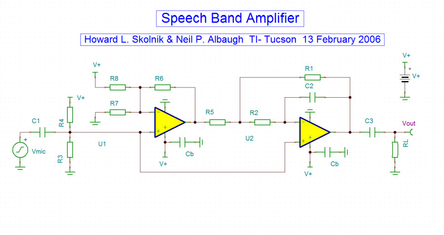
To provide practical insight, we will employ the schematic of a speech band amplifier from TINA Designsoft’s extensive circuit collection. Within this circuit, we will showcase the application of two opa345 operational amplifiers, offering a tangible and illustrative example for our exploration into the process of Importing SUBCKT PSpice Netlist into TINA.

In addition, another article that might interest you for importing PSPice models into TINA is this one


Speechbandamplifier


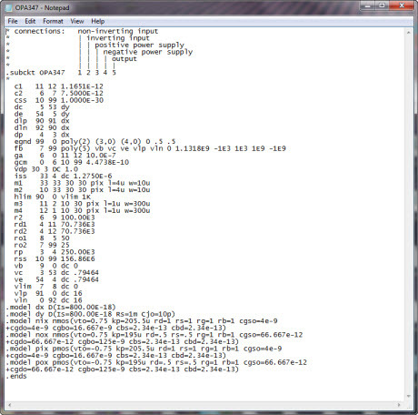
We want to replace the SPICE model of the opa345 with the following opa347 PSpice netlist, which includes the SUBCKT statement:


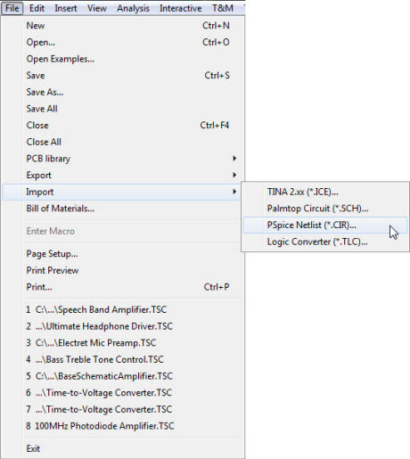
rename the .txt file as opa347.cir, then from the menu File, choose Import, PSpice Netlist (.CIR)


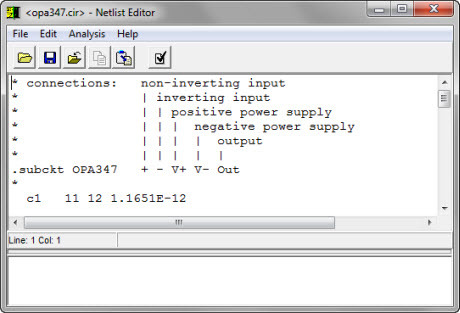
When you select the ‘opa347.cir’ file, the Netlist Editor window opens


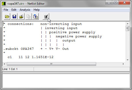
Click on the ‘Compile’ icon to verify the compatibility of SPICE statements with TINA. If there are no compatibility issues, a ‘Successfully completed’ message appears:


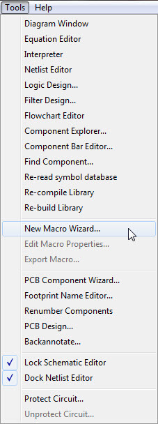
Close the Netlist Editor window, and then select ‘New Macro Wizard…’ from the ‘Tools’ menu


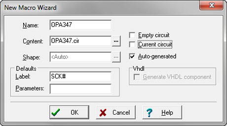
The “New Macro Wizard” window will appear. Enter “opa347” as the name and uncheck the “Current circuit” option. Now, you can select the file “opa347.cir” using the directory window. Make sure to uncheck “Auto-generated.”


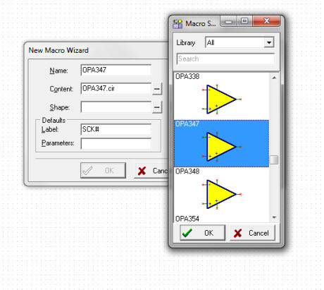
Click on the “Shape” ellipsis icon and choose a graphic symbol from the list. If there are no symbols that accurately represent our model, you can leave the check in the “Auto-generated” box:


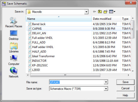
Save the macro (.TSM file) for example in the Macrolib directory:


TINA spice simulation

TINA SPICE Simulation

TINA is a versatile and user-friendly software tool that empowers users to design, simulate, and optimize electronic circuits with precision and efficiency. Its extensive feature set and TINA SPICE simulation capabilities make it a valuable resource in the field of electronics design and analysis. Here are some key characteristics of TINA:

  1. Intuitive User Interface: TINA boasts an intuitive and user-friendly interface, making it accessible to both beginners and experienced users. Its drag-and-drop functionality and interactive components simplify the process of designing and simulating circuits.
  2. Extensive Component Library: TINA provides an extensive library of electronic components, including semiconductors, passive components, and specialized devices. This library allows users to quickly build complex circuits by selecting and configuring components.
  3. SPICE Simulation Engine: TINA is powered by a robust SPICE (Simulation Program with Integrated Circuit Emphasis) simulation engine. This engine accurately models the behavior of electronic components and circuits, enabling users to predict how their designs will perform in the real world.
  4. Mixed-Signal Simulation: TINA supports mixed-signal simulation, allowing users to design and analyze circuits that combine analog and digital components. This is particularly useful for designing integrated systems.
  5. Parameter Sweeps and Optimization: Users can perform parameter sweeps and optimization studies to explore different design scenarios and find the optimal values for circuit parameters. This feature helps in fine-tuning designs for specific requirements.
  6. Interactive Waveform Analysis: TINA offers advanced waveform analysis tools that allow users to examine voltage and current waveforms at various points in the circuit. This helps in identifying and troubleshooting issues in the design.
  7. Interactive 3D PCB Design: TINA includes a 3D PCB design module that enables users to create and visualize printed circuit boards. This integration streamlines the transition from schematic design to PCB layout.
  8. Educational Resources: TINA is often used in educational settings due to its educational versions and resources. It provides a practical platform for learning electronics and circuit design principles.
  9. Integration with Microcontrollers: TINA can interface with various microcontrollers, making it suitable for embedded systems design. Users can simulate the interaction between microcontrollers and external circuitry.
  10. Custom Component Creation: For unique or specialized components, TINA allows users to create custom models, ensuring accurate simulation results for specific components or devices.

In this initial undertaking, we will commence our initial endeavors with TINA SPICE Simulation by formulating a three-stage BJT audio amplifier circuit. This preliminary endeavor aims to demonstrate the functionality of TINA while concurrently establishing a substantial groundwork for comprehending the complexities associated with electronic circuit design and simulation. Thus, we shall proceed to investigate the captivating domain of electronic design with TINA SPICE Simulation.

To delve deeper into the software’s features, you can refer to this article.


After running the program, we can see this window:


Globalview


On the components toolbar, there are devices in the ‘basic’ tab. Below the toolbar, when you select ‘semiconductors’ on the toolbar, several types of semiconductors appear:


Now select “Special”


And once again, we have a large number of devices to choose from. Let’s begin by selecting a resistor:


Place Resistors, to set value, double-click on one, and a parameters window will appear


ViaDesigner Video Tutorials

TopicVideo
Creating Tutorial Designs within ViaDesigner
Creating Simulation Models with the Datasheet Curve Tracer in ViaDesigner
“Do The Harlem Shake” Circuit to Detect Low Frequencies Audio Signals
Creating a VHDL model in ViaDesigner
Importing & Processing Oscilloscope Data in ViaDesigner Simulations
ESD Generator SPICE Simulation

ESD Generator SPICE Simulation.

In this article, we will explore the ESD Generator SPICE Simulation using an LTSpice model, shedding light on how this powerful tool can help analyze and enhance ESD protection strategies in electronic circuits.

ESD generator, also known as an “Electrostatic Discharge Generator,” is a device used in industrial and testing environments to simulate controlled and repeatable electrostatic discharges (ESD), which are sudden and brief electric currents that can damage or disrupt other electronic equipment. These generators are employed to test the resistance of electronic devices and circuits to simulated electrostatic discharges, assessing how these devices react and whether they are adequately protected against ESD-induced damage.

ESD generators can simulate different types of ESD pulses, such as those defined by various standards and applications. For example, some ESD generators can produce pulses that mimic the human body model (HBM), the machine model (MM), or the charged device model (CDM) of ESD. Some ESD generators can also produce pulses that comply with the requirements of the International Electrotechnical Commission (IEC) 61000-4-2 standard, which specifies the test levels and methods for evaluating the ESD immunity of electrical and electronic equipment.

To take your first steps with LTSpice simulation software, you can read this article.


Università Politecnica delle Marche, Ancona, Italy.

by

Ing. Luca Buccolini

A SIMPLE SPICE ESD GENERATOR CIRCUIT BASED ON IEC61000-4-2 STANDARD

WHAT IS ESD?

Static charge is an unbalanced electrical charge at rest. Typically, it is created by insulator surfaces rubbing together or pulling apart. One surface gains electrons, while the other surface loses electrons. This results in an unbalanced electrical condition known as static charge.

When a static charge moves from one surface to another, it becomes ESD. ESD is a miniature lightning bolt of charge that moves between two surfaces that have different potentials. It can occur only when the voltage differential between the two surfaces is sufficiently high to break down the dielectric strength of the medium separating the two surfaces.

When a static charge moves, it becomes a current that damages or destroys gate oxide, metallization, and junctions. ESD can occur in any one of four different ways: a charged body can touch an IC, a charged IC can touch a grounded surface, a charged machine can touch an IC, or an electrostatic field can induce a voltage across a dielectric sufficient to break it down


ESD STRESS MODELS

ESD can have serious detrimental effects on all semiconductor ICs and the system that contains them. Standards are developed to enhance the quality and reliability of ICs by ensuring all devices employed have undergone proper ESD design and testing, thereby, minimizing the detrimental effects of ESD. Three major stress methods are widely used in the industry today to describe uniform methods for establishing ESD withstand thresholds (highest passing level).


HUMAN BODY MODEL (HBM)

The HBM is a component level stress developed to simulate the action of a human body discharging accumulated static charge through a device to ground, and employs a series RC network consisting of a 100 pF capacitor and a 1500 Ohm resistor.


CHARGED DEVICE MODEL (CDM)

The CDM is a component level stress that simulates charging and discharging events that occur in production equipment and processes. Potential for CDM ESD events occur when there is metal-to-metal contact in manufacturing.


SYSTEM LEVEL ESD (IEC 61000-4-2)

The IEC system level ESD is a widely accepted European standard that defines an ESD event that is meant to be tested on actual end equipment to simulate a charged person or object discharging into electronic systems. The IEC standard defines an ESD stress that is much stronger than the component level ESD stresses defined by HBM and CDM.

The engineer must design following IEC 61000-4-2 standard to be able to declare the conformity CE (“Conformité Européenne”).

The ESD generator circuit realized in this work is compliant with ESD generator used in EMC laboratories to perform CE-conformity tests, thus a SPICE simulation can be used to test ESD-immunity solutions before circuit production.


IEC 61000-4-2 WAVEFORM CHARACTERISTICS

The standard accurately describe the characteristics and performances of the ESD generator as well as the current waveform parameters.

The ESD phenomenon is a very short but very strong current transient and is represented in Figure 1.


idealcontactESDwaveform

Figure 1. 61000-4-2 ideal contact ESD waveform at 4kV


This pulse is divided into two parts: The first peak, known as the “Initial Peak”, is caused by the discharge of the arm, and generates the maximum current. The second peak is caused by the discharge of the body. The rise time of the initial peak is between 0.6 ns and 1 ns, and its amplitude depends on the charging voltage of the ESD simulator.

The standard describe a formula and the mains current level of the waveform for different test level.

dischargeESDwaceform

Table 1 contact discharge current waveform parameters

Even though the IEC 61000-4-2 [2] include a simplified circuit of ESD generator, it is incompatible with the discharge current equation descripted in the standard and the waveform shown in Figure 1. A PSpice software simulation can prove this.


THE BASIC ESD GENERATOR MODEL

In order to run ESD stress simulation, an ESD-generator model was built. This can help engineers to test different solutions in a SPICE simulator to overcome strength over-voltages before realizing PCB circuit and test it against ESD.

The objective is to generate an ESD pulse that accurately corresponds to the current stress waveforms at various stress levels in accordance with the IEC 61000-4-2 specification.

The ESD can be simulated by two parallel R, L, C circuits with charged capacitors. The generator equivalent circuit is shown in Figure 2.

Here the standardized network elements of the ESD-generator are represented by R1 (330ohm) and C1 (150pF). The inductor L1 is considered to be the obligatory ground strap with the length of about 2 m. Physically the first peak of the pulse is shaped by additional lumped and parasitic elements around and in the tip of the ESD-generator [5].

Note that the values of R, L, and C for both branches are tweaked to correctly represent standard IEC stress waveform; “.ic V(c1)=4kV V(c2)=4kV” refers to the initial condition of the voltage on the capacitors for a 4kV zap.


Figure 2  The general equivalent circuit of basic IEC61000-4-2 generator model

LNA SPICE Simulation

LNA SPICE Simulation

In this article, we will delve into the fascinating world of LNA SPICE simulation, exploring how to replicate and analyze the behavior of a Low Noise Amplifier using two powerful tools: LTspice and Matlab. By simulating an LNA’s performance, we can gain valuable insights into its characteristics, such as gain, noise figure, and bandwidth, and optimize its configuration for specific applications. Let’s now delve into the potential of LNA SPICE simulation techniques to deepen our understanding and improve our design skills.

A crucial component in the field of electronic circuits, the Low Noise Amplifier (LNA) plays a pivotal role in various applications where signal amplification is essential while maintaining the integrity of the original signal quality. An LNA, as the name suggests, is primarily designed to amplify weak electrical signals with minimal additional noise, ensuring a high Signal-to-Noise Ratio (SNR). This key attribute makes LNAs indispensable in numerous fields, including wireless communications, radio astronomy, broadcasting, medical imaging, and telecommunications, to name a few.

The fundamental purpose of an LNA is to boost the strength of incoming signals without introducing significant noise that could degrade the overall performance. In wireless communication systems, for instance, an LNA is positioned at the front end of a receiver to amplify faint radio frequency (RF) signals received from antennas or other receiving devices. By doing so, it enhances the receiver’s sensitivity, allowing it to detect and process weak signals effectively. Similarly, in radio astronomy, where astronomers seek to capture faint celestial emissions, LNAs are utilized to amplify these extraterrestrial signals while preserving their inherent low noise characteristics.

One of the distinguishing features of an LNA is its ability to maintain a low noise figure. The noise figure quantifies the extent to which an amplifier adds noise to the signal, and a lower noise figure corresponds to a better LNA performance. LNAs are meticulously designed to minimize thermal noise and other forms of electronic noise, ensuring that the amplified signal remains as clean as possible. This is especially critical in scenarios where weak signals must be distinguished from background noise or interference.

For those unfamiliar with LTspice software, you can find an LTspice tutorial here.


Ventspils University College

Faculty of Information

by

Marcis Bleider


LOW NOISE PREAMPLIFIER FOR SATELLITE BASE STATION

In this article low noise preamplifiers (LNA) for satellite ground station (GS) of Ventspils University College (VUC) are designed creating possibility to repair and replace these commercially expensive, extremely sensitive and easily damageable units.

One of main purposes of GS of VUC is for communication with soon to be launched satellite Venta-1. GS will provide uplink/downlink communication channels for satellite telecommands and telemetry in 2m and 70cm amateur frequency bands as well as main data downlink channel in s-band. GS also will (and are) communicate with other student satellites orbiting in low earth orbits (LEO), like Estonian Estcube-1 and Danish AAUSat cubesat series.

Because it is not always possible to receive and decode all data packets in particular satellite pass, skipped packets should be retransmitted in next pass – there are only few passes with acceptable elevation per day. Even though we are located very close to Estonia and Denmark and we are receiving same data as their ground station, our received data may contain packets that main station failed to receive, so data could be forwarded to main mission control center resulting in higher throughput. In any case, our station could be used as remote backup station, increasing redundancy of communication system.

Signals from satellites can be exquisitely weak, which means they need as much amplification as possible to be readable. The way to ensure that you have a useable received signal is to install a receive LNA at the antenna [1]. This is a high gain, low-noise amplifier with a frequency response tailored for one band only. Even though equipment of GS  includes a few such preamplifiers, these units are very expensive, for example 2m/70cm band Kuhne Electronic LNAs costs 224 EUR per unit  [6].

Because  LNA  is  very  sensitive device  it  is  very  prone  to  damage  by lightening induced voltage spikes, static electricity and even by strong nearby radio transmission  signals.  Of  course  by  correct  system  setup,  like  switchover  relays, damage risk is greatly reduced, but LNA is still one of weakest link of the system in respect to failing. If device fails, it would be very non-economical to by new one each time, not to mention that it would not be possible to repair or replace it right away to reestablish operation of communication system as fast as possible.

In this work, theory of operation and typical design methods of LNAs are researched, and example design and testing procedure is described. For reference, two 70cm band LNAs are designed, built, tested and performance-price compared. In this particular paper, one 70cm LNA is designed and simulated with MATLAB using scattering parameter (s-parameter) and Smith chart method and LTSPICE software. It should be noted that preceding description is very superficial and only presentative.

The RF amplifier which is at the input stage of the receiver is usually designed to give the best gain parameter and the least noise. It is done so for the reason that the noise and distortion parameters would get depressed in the later stages of the receiver system [3]. Friis’s formula is used to calculate the total noise factor of a cascade of stages, each with its own noise factor and gain (assuming that the impedances are matched at each stage) [7]. The total noise factor can then be used to calculate the total noise figure is given in equation 1.


Ftotal

(1)


 Where


LTspice Video Tutorials

TopicVideo
Getting started with LTspice simulation software
Operating Point Analysis with LTspice, part 1
Operating Point Analysis with LTspice, part 2
Performing a Transient Analysis with LTspice
Tracing of the Simulation results in LTspice, part 1
Tracing of the Simulation results in LTspice, part 2
Tracing of the Simulation results in LTspice, part 3
Adding a model in LTspice
LTspice using Mac
LTspice Tutorial

LTspice Tutorial

Welcome to this LTspice tutorial! LTspice, developed by Linear Technology (now part of Analog Devices), is a robust and highly versatile SPICE-based electronic circuit simulation software that has become an invaluable tool for engineers, students, and hobbyists alike. In this tutorial, we will explore the remarkable features of LTspice that empower users to design, analyze, and refine electronic circuits with precision and efficiency.

One of the standout features of LTspice is its extensive library of components. This library includes a comprehensive selection of analog and digital components, such as resistors, capacitors, inductors, transistors, op-amps, microcontrollers, and more. This expansive library ensures that users have access to a wide range of components to accurately model their circuits. Furthermore, we will show you how to add custom components to the library, enabling you to work with specialized or proprietary components specific to your projects.

Advanced simulation capabilities are another key strength of LTspice. It employs a powerful simulation engine capable of handling both transient and steady-state analyses. Through this tutorial, you will learn how to perform transient analysis to observe how a circuit responds over time, making it ideal for studying transient phenomena like start-up behavior and signal processing. You will also master steady-state analysis, allowing for the assessment of a circuit’s behavior under stable conditions, which is crucial for understanding its performance in practical applications.

LTspice’s ability to perform AC analysis is particularly useful for designing and analyzing circuits that operate with alternating currents. We will guide you through using this feature to evaluate the frequency response of a circuit, helping you optimize filter designs, amplifier performance, and more. Moreover, we will delve into Monte Carlo analysis and worst-case analysis tools, allowing you to assess the impact of component tolerances and variations on circuit performance—essential for designing robust circuits that can withstand real-world variations in component values.

The software’s user-friendly interface simplifies the process of schematic capture and modification. Throughout this tutorial, we will demonstrate how to easily draw circuit schematics and make changes with drag-and-drop functionality. The intuitive interface also allows for quick connections between components and nodes, reducing the time required to create complex circuit designs.

LTspice’s waveform analysis capabilities are indispensable for evaluating circuit behavior. You will learn how to plot waveforms, measure signal parameters, and perform Fourier analysis to examine frequency components in signals. This functionality is essential for troubleshooting and optimizing circuit designs.

One of the standout advantages of LTspice is its cost-effectiveness—it’s available for free! We will emphasize this throughout the tutorial, making it accessible to a wide audience, including students and hobbyists. Rest assured, this affordability does not compromise the quality or depth of its simulation capabilities, making it a top choice for educational institutions and professionals alike.

In conclusion, this LTspice tutorial aims to equip you with the knowledge and skills needed to harness the full potential of this remarkable software tool. Its extensive component library, advanced simulation capabilities, user-friendly interface, and affordability make it an indispensable resource for engineers and electronics enthusiasts. Whether you are a seasoned professional or a student learning the ropes of circuit design, LTspice provides the tools and capabilities needed to bring your electronic projects to life. So, let’s dive in and explore the world of LTspice together!


With this LTspice tutorial, we see how how to use LTspice for a Switching Mode Power Supply (SMPS) simulation:


After installing LTspice, run the software:


LtspiceIV


To initiate a new project, choose “New Schematic” and activate the grid


At the top toolbar, you can find the buttons to place all devices:


Select the Component Icon:


Getting Started with Micro-Cap SPICE software

Simple step by step guide for getting immediately operative with Micro-Cap.We ‘ll design a transistor BJT that works as amplifier.

This is an overview of Micro-Cap IDE

Microcapglobalview

On the top toolbar we can find the main tools and components button to draw any projects

On the left panel are available the models libraries

Expanding Analog Library we can find the model of BJT BC548B