
Next, after cascading shunt resistor at the output of amplifier, constant gain, noise figure and input/output stability circles are drawn in figure 4. Input and output stability circles lays outside of smith chart, which means that amplifier is unconditionally stable or stable with all source and load impedances.
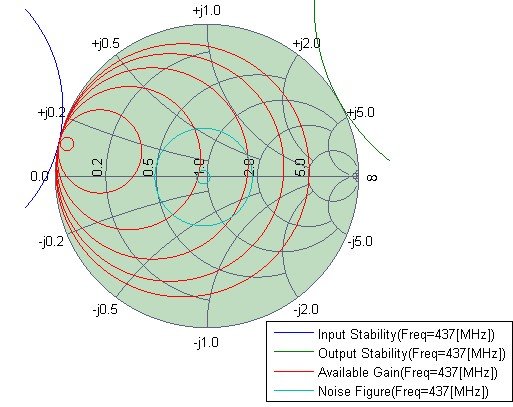
Figure 4. Constant gain, noise figure and input/output stability circles.
Using figure above, source reflection coefficient

and load reflection coefficient

are found which gives optimal compromise between gain and noise figure.
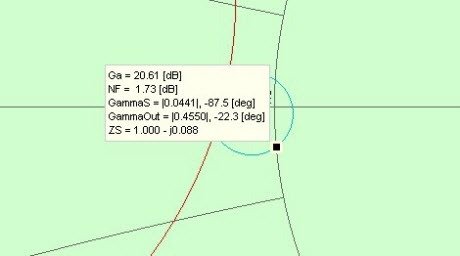
Figure 5. Optimal input and output reflection coefficients.
Reflection coefficients are converted to impedances which should be conjugate matched to 50Ω impedance [10]. To do this, constant impedance and conductance circles, which crosses points of the reflection coefficient to be matched and center of Smith chart. Selected matching network topology is high-pass L network or one series capacitor and shunt inductor:
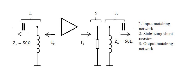
Figure 6. Amplifier block diagram.
Input matching is simple – just series capacitor with normalized impedance of 0.088 (conjugate of -0.088 in figure 7) which is 82pF at 437MHz and 50Ω characteristic impedance. Similarly, normalized values of output matching network are found, which are 1.259 (distance between chart center and cross point in figure 7) for series capacitor and 0.6465 (distance between cross point and the reflection coefficient in figure 7) for shunt inductance. Absolute values are respectively 5.8pF and 28nH. 5.6pF and 30nH are selected as standard values.
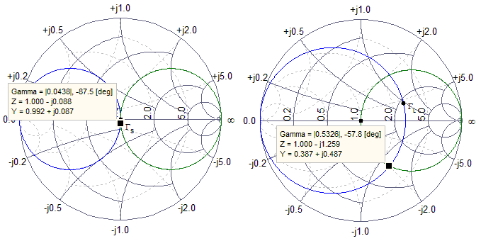
Figure 7. Input and output matching L network value determination.
Now design can be verified by cascading matching networks, amplifier and stabilization resistor and plotting gain and noise figure versus frequency.
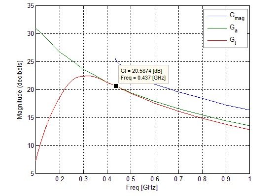
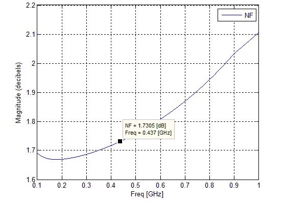
Figure 8. Gain and noise figure after matching.
As it can be seen from figure 8, after matching, gain at 437MHz is 20.6dB and noise figure is 1.7dB. Also Gmag now exists at 437MHz – amplifier is unconditionally stable.
Final circuit and printed circuit board is shown in figure 9. Upper lead of L1 is AC grounded by C3, so output matching network corresponds to block diagram in figure 6. Potentiometer R3 is used to precisely trim the bias current.
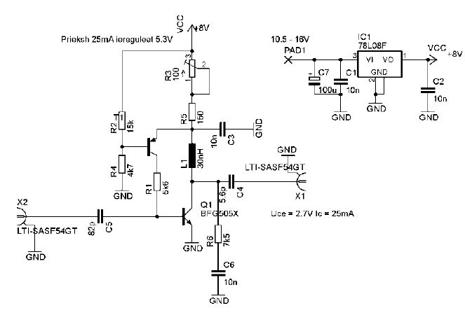
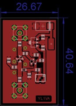
Figure 9. Final circuit and PCB.
After building this circuit, measurements, like gain-versus-frequency plot, noise figure, third order interception point will be carried out. All the necessary equipment, like signal generators, network/spectrum analyzers, noise sources are available at laboratories of VUC and VSRC. Operating such equipment and doing this kind of testing
also would be important section of final paper.
References:
[1] The American Radio Relay League, The ARRL handbook for Radio
Communictations, 2013. ISBN: 978-0-87259-405-0
[2] Agilent Technologies, Practical RF Amplifier Design Using the Available Gain Procedure and the Advanced Design System EM/Circuit Co-Simulation Capability, 2009
[3] Kaja Najumudeen & Charles, Active antenna amplifier, 2009 [4] Chris Bowick, RF Circuit Design, 1982. ISBN 0-7506-9946-9
[5] Avago, General Purpose, Low Noise NPN Silicon Bipolar Transistors AT-
41511, AT-41533, 2009. [Accessed 11.01.2014]. Available: http://www.avagotech.com/pages/en/rf_microwave/transistors/silicon_bipolar/ at-41511/.
[6] Kuhne Electronic, Pricelist for Amateur Radio Components, [Accessed
11.01.2014]. Available: http://www.kuhne- electronic.de/fileadmin/userfiles/_pdf/preisliste/kuhne_pricelist.pdf
[7] Wikipedia, Friis formulas for noise, [Accessed 11.01.2014]. Available:
http://en.wikipedia.org/wiki/Friis_formulas_for_noise
[attachments title=”low noise preamlifier files” logged_users=2 include=”490″]