An important consequence of this formula is that the overall noise figure of a radio receiver is primarily established by the noise figure of its first amplifying stage. Subsequent stages have a diminishing effect on signal-to-noise ratio. The overall noise factor is dominated by the noise factor of the LNA, if the gain is sufficiently high. Besides gain and noise figure there are other important characteristics of LNA, like bandwidth, third order intercept point (IP3), temperature range.
In subsequent design, the selected RF device is general purpose, low noise NPN silicon bipolar transistor AT-41511 [5]. It has reasonably high gain of 15. 5dB and low noise figure of 1dB at 900MHz working frequency. At design frequency of 437MHz these parameters will be better. One of reasons why this particular device was selected was good documentations, in particular, at has pre-measured s-parameter tables, which includes design frequency of interest. Other reason is its low cost – it costs only a few cents, which makes it perfect for experimentation and prototyping, as this particular design is just experiment to learn basics of design, building, measuring and analyzing LNA devices. The final design would use much better (a bit costlier) device like ATF-54143, which has parameters capable to compete with commercial LNAs like Kuhne Electronics ones.
The first design step is choosing of DC bias point and bias network. It is very important, because s-parameters thereby AC characteristics depend on DC bias, more accurately particular collector current Ic and collector-emitter voltage Uce. It is compromise of gain, noise figure and available supply voltage/current – more collector current results in more noise but higher gain and vice versa. It is the same case with Uce also. The selected bias
point is Ic = 25mA and Uc = 2.7V, because lower Uce allows to use lower supply voltage which is nominal 13.8V. More voltage “headroom” is needed for voltage regulator dropout and larger output dynamic range. Other important aspect is bias network selection. Since it is planned to mount LNA on antenna mast, it is important to have stable bias in wide temperature range. Three bias networks are analyzed using LTSPICE. Selected power supply voltage is 8V.

Figure 1. Three types of candidate bias networks.
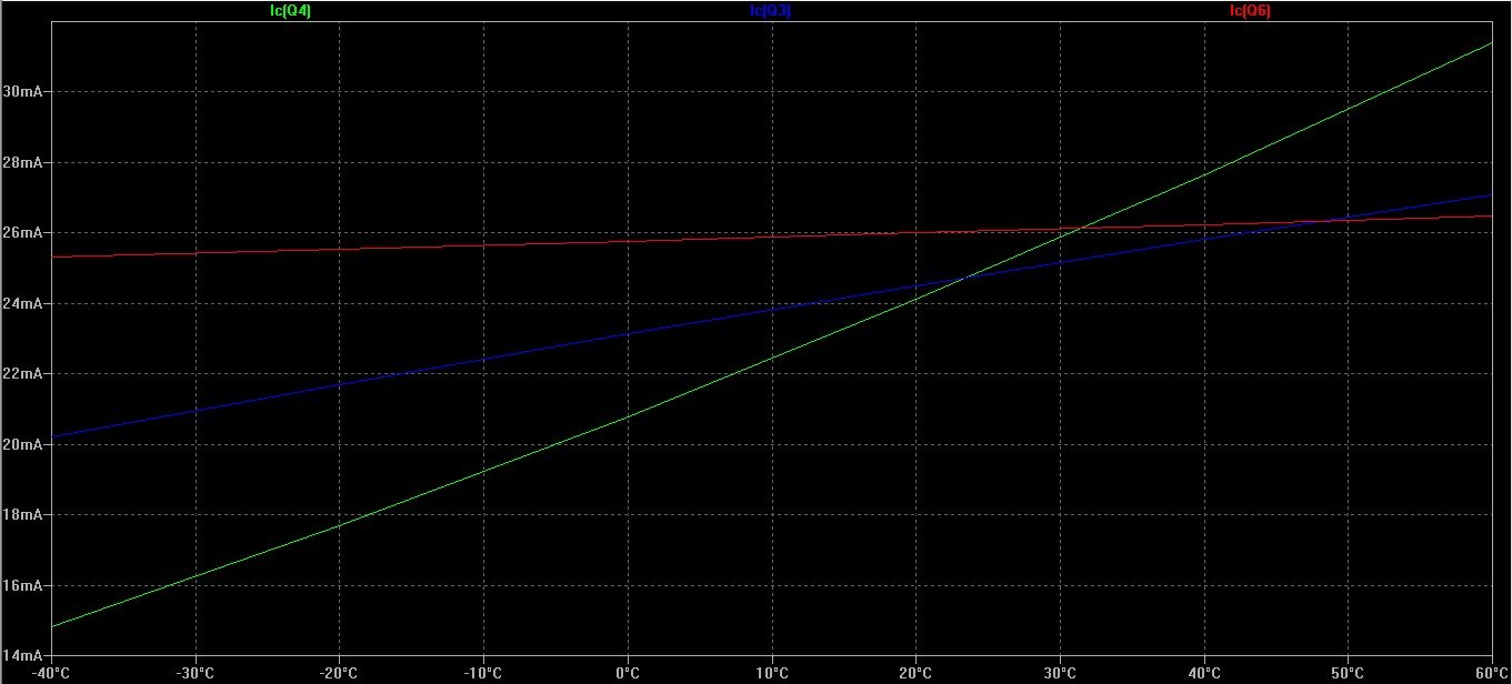
The network 1 has grounded emitter and bias point is set by voltage divider R13 – R14 as well as R12. Second one has addition of emitter resistor, as result simple negative feedback is obtained – if Ic tends to increase, emitter voltage increases, decreasing base-emitter voltage as result Ic decreases and vice versa. Third network is so called active biasing. Q7, R17, R15 and R5 forms current source, so that base current of Q6 (main transistor) is controlled so that voltage on R5 is constant – that means current also remains constant. All three network bias point dependency of temperature is simulated in range from -40 to +60 °C.

Figure 2. Collector current dependency of temperature.
From figure 2 is obvious that network 1 is useless in wide temperature range. Second one is better, but it has one lack, particularly it doesn’t have grounded emitter at signal frequencies – it is necessary to use shunt capacitor which can degrade performance especially at 437MHz center frequency. Third network clearly performs the best so it is selected for design. Addition of few resistors and low cost transistor costs no more than few cents.
Next step is to design input and output matching networks. For this task manufacturers provided S-parameter file (Also known as Touchstone file) is used. S – Parameters describe device using measured input and output reflection coefficients (S11 and S22 ), forward transmission coefficient or gain S21, and reverse transmission coefficient S12 [4]. All four parameters are complex quantities. As design environment MATLAB RF Toolbox is used and matching networks are calculated using Smith chart method. Smith chart is very useful tool for such purposes as it simultaneously can display complex impedances, reflection coefficients, S – parameters, noise figure and gain circles and many more.
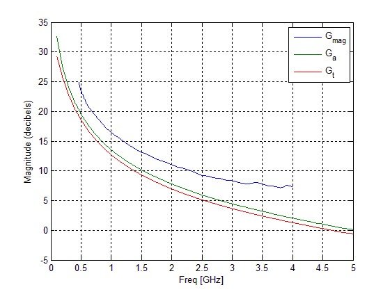
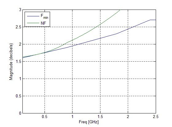
First available gain Ga (Available gain if output is matched), Gmag (Maximum available gain if both input and output are matched), Gt (Transducer gain or unmatched device gain) and noise figure before matching are plotted.


Figure 3. Gain and noise figure before matching
It can be seen that Gmag doesn’t exist for 437MHz, which means that amplifier is potentially unstable at that frequency and needs to be stabilized. One way to stabilize an amplifier is to cascade a shunt resistor at the output of the amplifier. Calculated shunt resistor has value 7.64KΩ. 7.5KΩ is used, which is standard value.

