3. Simulation of output charecteristics of JFET.
PSPICE coding:
*OUTPUT OR DRAIN CHARACTERISTIC OF NJFET
VGS 1 0 DC 0V
VDD 2 0 DC 12
J1 2 1 0 JMOD
.MODEL JMOD NJF(IS=100E-14 RD=10 RS=10 BETA=1E-3 VTO=-5)
.DC VDD 0V 12V .2V VGS 0V -4V 1V
.OP
.PROBE
.END
GRAPHICAL ANALYZER:

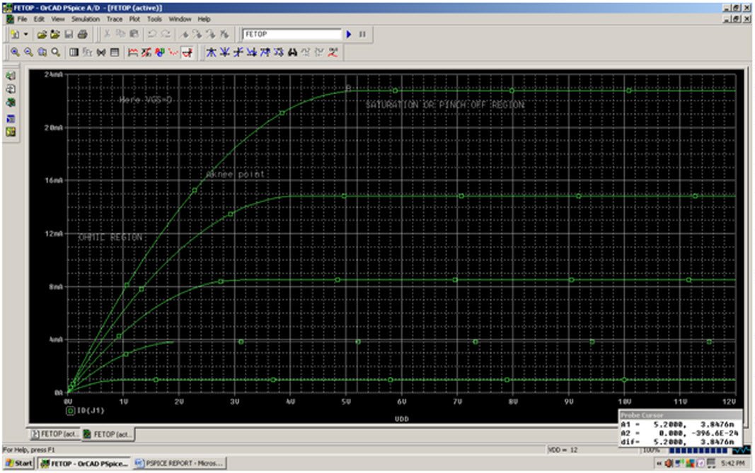
CONCLUSION: When VDS=0 then ID=0 as VDS is increased then IDS is also increased upto a point A which is knee point means in this region JFET behave like a register so its known as OHMIC REGION.
*Point B is known as pinch off point from A to B VDS progressively increased with ID.
*After point AB JFET enters saturation or amplifier region because VDS is further increased with channel registence in such a way that ID remains constant.
4. Simulation of transfer characteristic of n channel JFET.
PSPICE CODING:
*TRANSFER CHARCTERISTIC OF JFET
VGS 1 0 DC 0V
VDD 2 0 DC 10V
J1 2 1 0 JMOD
.MODEL JMOD NJF(IS=100E-14 RD=10V RS=10V BETA=1E-3 VTO=-5)
.DC VGS 0V -5V .5V
.OP
.PLOT DC I(VGS)
.PROBE
.END
GRAPHICAAL ANALYZER:

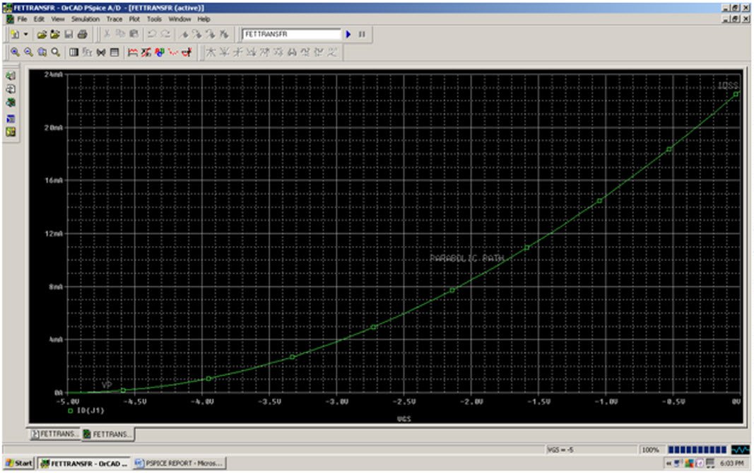
CONCLUSION: It can be concluded from the graph that when VGS=0 then ID=IDSS and when ID=0 then VGS=VP and graph is a part of the parabola.
5. Simulation of JFET Amplifier for frequency and transient analysis.
*FREQUENCY(only at 1 point) N TRANSIENT RESPONCE OF JFET AMPLFR
VIN 1 0 AC 0.5V SIN(0 0.5V 1KHZ)
VDD 7 0 DC 20V
VI 8 2 DC 0V
VX 6 9 DC 0V
RRS 1 8 50
RG 3 0 .5MEG
RD 7 4 3.5K
RS 5 0 1.5K
RL 9 0 20K
C1 2 3 10UF
C2 4 6 1UF
CS 5 0 10UF
J1 4 3 5 JMOD
.MODEL JMOD NJF(IS=100E-14 RD=10 RS=10 BETA=1E-3 CGD=5PF CGS=1PF VTO=-5V)
.AC LIN 1 1KHZ 1KHZ
.TRAN/OP 10US 1MS
.OP
.PRINT AC VM(6) VP(6) IM(RRS) IP(RRS) IM(RL) IP(RL)
.PROBE
.END
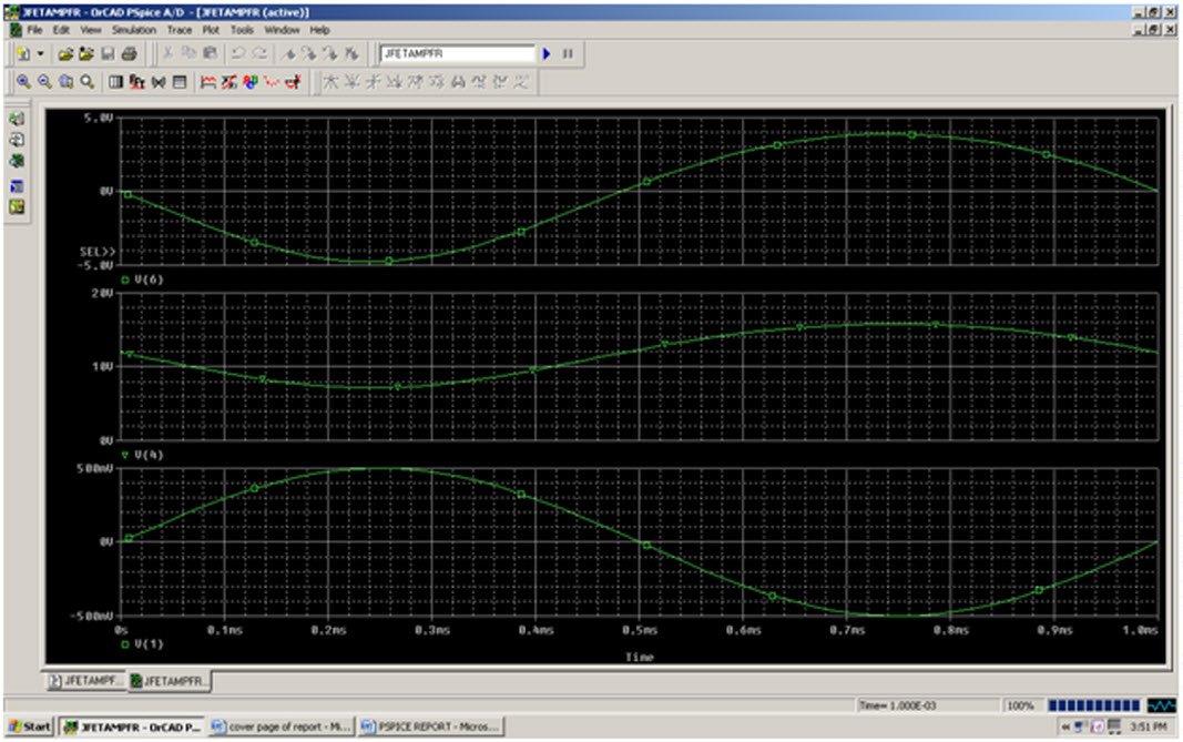
GRAPHICAL ANALYZER FOR TRANSIENT ANALYSIS:

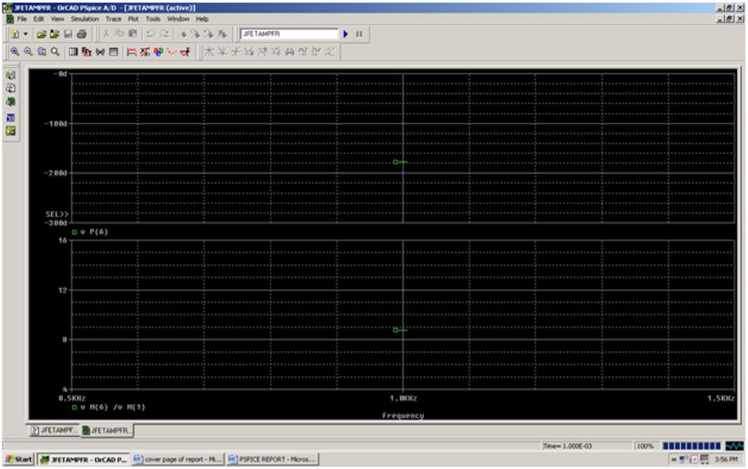
GRAPHICAL ANALYSIS FOR FREQUENCY ANALYSIS (only for one point):

