5. Windings: supports, insulation and wires.
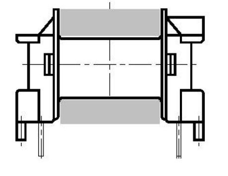
Figure 4 – Coil former for horizontal mounting.
After the calculation of the number of turns we must now determine on what make the windings, how and with what
On what
Normally each type of ferrite is associated with a support (coil formers) identificable from the catalog. They are normally made of plastic material (phenolformaldehyde PH [2], polyterephthalate GFR [1]). It ‘s usually present with a single groove on which are placed the windings of the primary/ies and the secondary/ies. The metal pins allow both anchoring of the wires of the windings, and the mechanical and electrical
connection of the transformer to the board.
We can choose the vertical support mounting, direction in which the transformer is mainly developed, or the horizontal support mounting. In Figure 4 is shown the design of a horizontal support mounting, the grey area represents the theoretical section available for the windings, but we ‘ll see later that this is true only for low voltage applications. From the catalog is possible to obtain, in addition to size, other parameters relating to the support as the area available for the windings AN and the average length of a loop IN.
In the applications where the primary of the transformer is directly connected to the grid the standard EN60950 requires compliance of minimum distances between the windings [2] [4] [9] [10]. It’s defines as “Creepage distance” the shortest surface path between two different electrical circuits. In the applications with the primary connected to the grid 230Vac (about 325Vcc), the value of the minimum surface distance is 4 mm, for the normal insulation, while for the reinforced insulation we have to double the value, then 8mm.
In the realization of the windings, it will not be possible to use the entire width of the support, but must be left side margins of 4 mm, for the reinforced insulation, as shown in Figure 5.
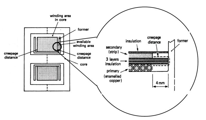
Figure 5 – Schematic representation of a section of a transformer with particular creepage distance (Soft FERRITES – Data Handbook, Philips Components).
How
In the transformer for switching power supplies, in addition to the losses in the ferrite, for the hysteresis and eddy currents, and in the copper, due to the electrical resistance of the conductor, there are other elements that create considerable problems, among them, the parasitic capacitance and inductance.The parasitic capacitance occurs between turns, between layer and layer and especially between primary and secondary/ies.
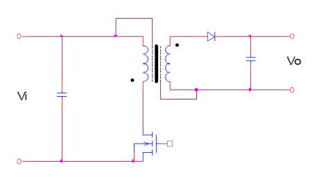
Figure 6 – Example of an electrostatic shield between primary and secondary.
It ‘s possible to study the phenomenon from an analytical point of view and derive the model that describes the coupling capacitance of the windings [6]. The need to reduce the effects of capacitive coupling between different circuits can be deal with the addition of electrostatic shields, as shown in Figure 7. In this way, in addition to decrease the coupling capacitance between primary and secondary, we also get the benefit from the reduction of electromagnetic emissions at the secondary (EMI). The shields are made by wrapping strips of conductive material (aluminum or copper) between the windings, it should be noted that they mustn’ t short the coils, and that between the shield and the winding is necessary to ensure the insulation under the rules mentioned above.
The parasitic inductance derives by the fact that not all the flux lines are concatenated between primary and secondary/ies, but there will be always a leakage flux, despite the geometries of the cores are designed to reduce it. The parasitic inductance value can be limited dividing the primary in two or more layers and winding the secondary in the middle [3] [6]. The considerations previously made for the insulation between primary and secondary remain valid. In order to maintain low the parasitic inductance value, we have to avoid, where possible, the realization of the air gap through interposition of shims on the external columns of the half-cores. It is preferable to use the specific half-cores made with the central column shorter.
The parasitic inductance value can be measured, this is done by measuring the inductance of the primary with the secondary closed in short-circuit, while to measure the inductance of the primary, the secondary must be left open. If possible it is good practice to take measurements at the same frequency for which the transformer is designed. The ratio between the parasitic inductance value and the inductance of the primary should be less than 1-2%. It can also be estimated with the following formula:

where:
Lsigma: Leakage inductance in H
mu0: magnetic constant 12.56 * 10-9 H/cm
NP: number of turns in the primary
ln: average length of the coil in cm
w: maximum width of the winding in cm
x: thickness of the insulation separation between primary and secondary in cm
y: depth of the windings in cm
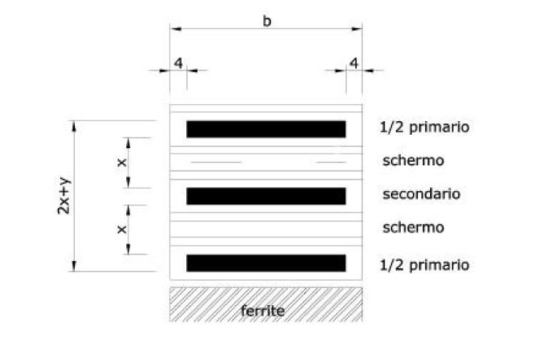
Figure 7 – transformer section: primary on two layers with secondary interposed.
With what
The conductors commonly used for transformers of this type are copper wires insulated with a plastic film. They are called magnet wires, because they are used in circuits to produce magnetic fields (transformers, inductors, relays, etc..). The main parameters that characterize these conductors are the gauge or nominal diameter, the type of insulation and/or its thickness, the thermal class of insulation and other marginal characteristics such as the color of the insulator, the weldability etc. The following table taken from [15] shows a list of names of families of enamelled copper wires, indicates the availability in the round or square/rectangular sections, the maximum operating temperature. The number NEMA (National Electrical Manufacturers Association) refers to a list published by NEMA that standardizes the sizes of the conductors in the USA.

Table 4 – Different types of enamelled winding wires of PIREMAG.
The Table 10 gives the nominal dimensions of the enamelled copper wires, with the maximum and minimum variations of the gauge due to the coating of the insulating film. The gauge of the conductors are referred to as AWG (American Wire Gauge) where a smaller number corresponds a larger wire section.
To convert AWG to inches or to millimeters you can use the tables, or you can use the following formulas:
conversion from AWG to nominal diameter in inches:

(0.27)
AWG to mm conversion:

(0.28)
Skin effect and proximity effect.
To determine the copper losses, consider the electrical resistance of the conductor when the current flows in it.
In estimating the value of the electrical resistance we have assumed that the current is distributed uniformly over the entire section of the conductor. Working at relatively high frequencies is now essential to consider two phenomena, the skin effect and proximity effect. The first, causes the innermost areas of the conductor exhibit a reactance greater than the peripheral ones, therefore the distribution of the current in the conductor cross section will not be homogeneous and and the current will have a density higher near the surface.
The proximity effect due to the field generated by adjacent conductors further contributes to a distribution of the current far from uniform. Not the whole section of the conductor is used, then the previously calculated value of resistance with DC current, will have to be corrected.
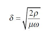
The formula (0.29) allows us to calculate the depth of penetration below which the current density is reduced of 1/e (about 37%) [8]
(0.29)
where:
delta: penetration depth in m
ro: specific resistivity (copper at 20 C 0.0172) in Ohm mm^2
mu: permeability (copper about 1) in H/m
omega: pulsation in rad
From (0.29) for copper at 20 °C (ro = 0.0172, mu = 1) is

(0.30)
where:
delta: penetration depth in mm
f: frequency in Hz
Therefore we can estimate the value of resistance in AC with the following formula [8]

(0.31)
where:
r: radius of the cylindrical conductor in mm
The procedure described above for the determination of losses in the copper, is not the most accurate but provides good results. Other approaches are possible, much more heavy from a point of view of calculation, where in the first instance, it’ s calculated the ratio between the value of the winding resistance in AC and the value of resistance in DC. To determine the amount of losses for a square wave it’s first calculated the value of Rac, then are summed products Rac * (In)^2 where In is the current value of the fundamental frequency and its harmonics.
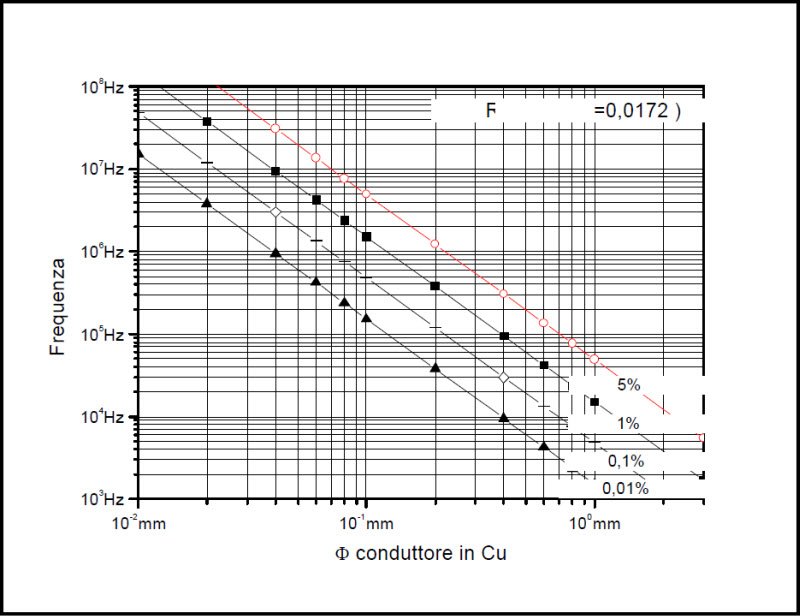
Figure 8 – Increase in percentage of the resistance of the wire depending on the diameter and frequency.
The graph shown in Figure 8, shows the percentage increase of the resistance of the copper conductor full in function of its diameter and frequency. The use of combinations Frequency/diameter such as to fall below the area bounded by the straight line relative to an increase of 0.1% of the resistance for the skin effect, represents the optimal zone. The area above the line on the increase of 5% must be avoided.
So in order to increase the efficiency of the transformer we have to use wires of contained dimensions, if the value of the current is high, to keep to an acceptable value the current density we can use multiple wires in parallel. A simplification in the implementation of the windings can be achieved by using Litz wire. It is composed of more enamelled copper wires, then with an insulating coating on the surface, appropriately helically wound and enclosed in a sheath. In this way we can add the sections of each individual conductor while maintaining modest increases in resistance in AC because the size of each single conductor are small.
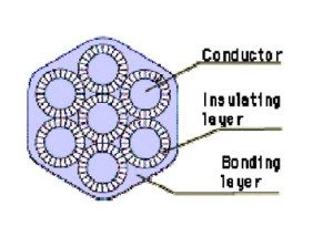
The AWG number, referred to Litz wire, identifies the equivalent section conductor, which may be obtained with different combinations, for example Litz wire AWG 20, which is equivalent to a conductor section of 0.519 mm^2 (804 mils^2), we can realize it with 4 conductors AWG26, or 5* AWG27 or 6*AWG28, or 8*AWG29, 10 * AWG30, 13*AWG31, 16 * AWG32, 20 * AWG33. The equivalent section remains approximately the same, change the size of the individual conductors, so we can increase the efficiency of the transformer choosing the best combination as a function of the switching frequency.
It should be recalled that if on the one hand the use of Litz wire produces several advantages, as every coin there is also its reverse. The value of DC resistance, at equal length, increases slightly when compared with a unic conductor of same cross section. This is because the individual wires that implement the Litz wire are spirally wound, then the length is greater. The resistance values in ohms per 1000 feet for different types of Litz wire are shown in Table 7, Table 8 and Table 9 in the appendix. Another drawback encountered with the use of Litz wire is a worst size factor (ratio between the copper surface and size area), in fact increase the interstices between wires. The illustrations shown in the appendix show different possibilities of assembly of the “rope” of conductors with which Litz wires are made, in particular we can note that a rectangular cross-section is possible (type 7 and 8), optimized as coefficient of space size for secondary low voltage and high current.
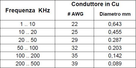
Table 5 shows the maximum dimensions of individual solid copper conductors for different frequencies, so that the increase of resistance, then the losses, for skin effect are lower than one per thousand. For Litz wires, the manufacturers provide tables of recommended values with the size of the individual wires much smaller than that shown above (see Table 6 in Appendix).
